

System integrators, panel builders, and procurement teams rarely fail because they lack a power supply topology. They lose time—and budget. When a seemingly functional prototype fails conducted emissions testing by 20 dB at an accredited EMC laboratory. Which forcing a complete PCB layout redesign weeks before the scheduled product launch. The root cause is rarely the circuit design itself. It is almost always the physical implementation—the component placement, the trace routing, the grounding scheme. Which determines whether a power supply meets its efficiency, thermal, and electromagnetic compatibility targets.
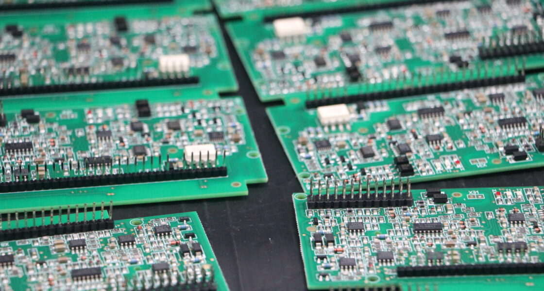
TPS Elektronik’s custom power supply circuit board design service eliminates this risk at the layout stage. By integrating DFM (Design for Manufacturability) analysis and EMC‑aware layout techniques from the first component placement, TPS delivers power supply PCBs that are not only electrically correct but also optimized for high‑volume production and designed to pass EMC compliance testing the first time. This service is purpose‑built for compact switch‑mode power supplies and DC‑DC converters where space constraints, thermal management, and EMI control must be balanced simultaneously.
1. Why power supply circuit board design demands a specialist approach
A switch‑mode power supply (SMPS) PCB is fundamentally different from a digital logic board. While a microcontroller board routes low‑current signals between ICs, a power supply board must manage high‑voltage isolation, high‑current paths, high‑frequency switching nodes. And sensitive feedback networks—all on the same substrate. A poorly placed switching node can radiate harmonics into the MHz range. Which coupling into nearby signal traces or, worse, into the input leads and back onto the AC mains. The result is a conducted emissions failure that no amount of post‑design filtering can economically fix.
Specialist power supply circuit board requires understanding not only the circuit topology but also the parasitic elements that the layout itself introduces. Every trace is an inductor; every plane gap is a slot antenna. Every via adds impedance in the high‑current path. The TPS design team brings decades of combined experience in power electronics to every layout. Which ensuring that the physical board faithfully reproduces the intended circuit behavior. This expertise embedded within TPS’s broader EMS capabilities, as detailed in the Electronic Manufacturing Services complete guide.
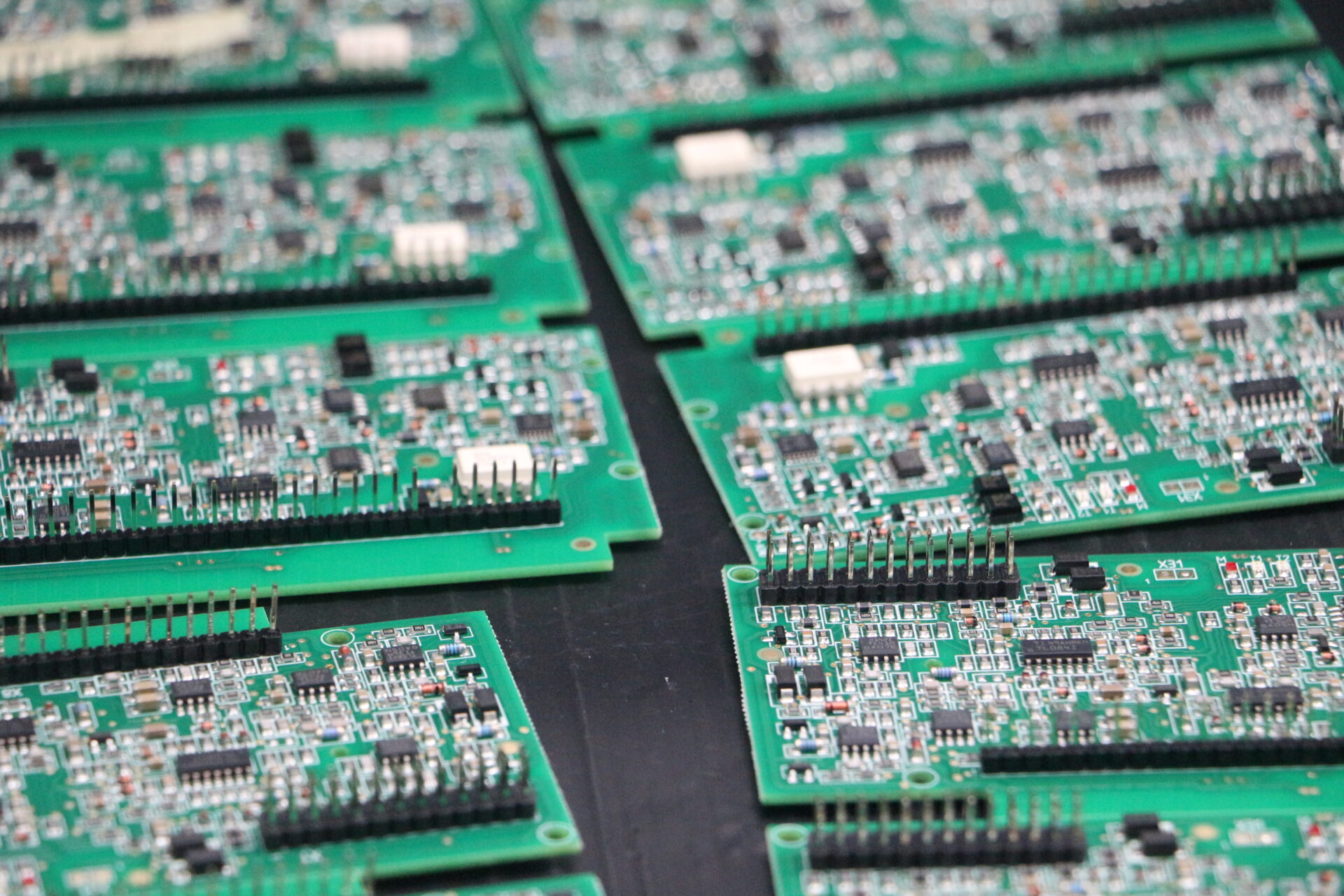
2. TPS power supply circuit board design methodology
TPS follows a structured design methodology that integrates electrical, thermal, and manufacturability considerations from the very first step. The process tailored to the specific topology. Whether a simple flyback, a resonant LLC converter, or a multi‑phase buck regulator. And to the target power level and form factor.
2.1 Schematic capture and component selection
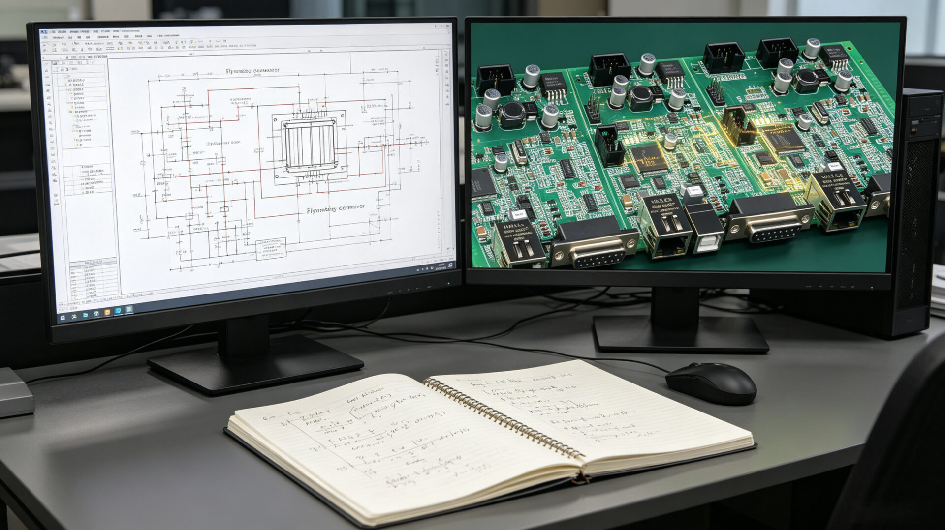
The design process begins with schematic capture, where every component selected not only for its electrical parameters but also for its availability, cost, and footprint compatibility with the target PCB density. TPS engineers work from the customer’s specification—input voltage range, output voltage and current, efficiency target, and any required isolation voltage. Which to propose the optimal topology and key component selections. This phase includes a review of the bill of materials (BOM) against TPS’s approved vendor list, mitigating the risk of selecting components that are on allocation or nearing end‑of‑life. For a deeper look at how component selection integrates with assembly. Which refer to the guide on electronic components and PCB assembly testing.
2.2 EMC‑aware layout: loops, planes, and isolation
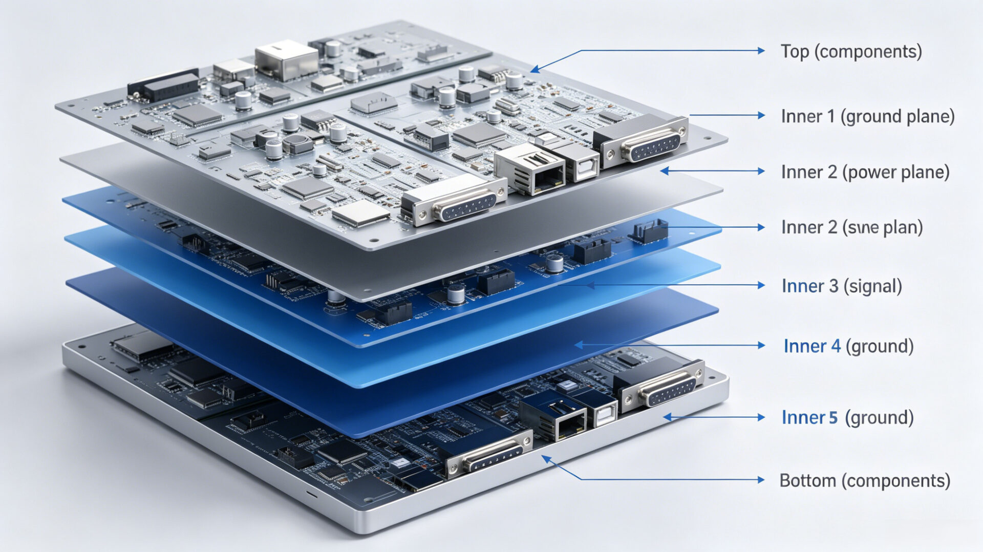
The physical layout is the single most influential factor in the EMC performance of a power supply. TPS engineers apply proven layout principles to minimize electromagnetic interference at its source. The primary strategy is to minimize the area of all high‑frequency switching loops. The tight physical loops formed by the input capacitor, the switching transistor, and the transformer primary or inductor. TPS achieves this through careful component placement, the use of unbroken ground planes on inner layers. And by keeping the switching node as compact as possible. The primary and secondary sides separated by a clear isolation barrier, with creepage and clearance distances verified against the requirements of IEC 62368‑1. The ground plane is never split arbitrarily; instead, components placed to control the return current paths. The critical feedback trace routed away from high‑dv/dt nodes to avoid capacitive noise pickup. These techniques further complemented by the assembly capabilities described in our guide on SMD PCB assembly and THT assembly.
2.3 Thermal management in dense power supply PCBs
Power semiconductors and magnetics generate significant heat, and in a compact design, this heat must be managed without compromising electrical performance. TPS designers use the PCB copper itself as a heat spreader, specifying heavy copper layers (typically 70 µm or 105 µm. And up to 210 µm for extreme cases) for the high‑current power paths and the areas under power devices. Thermal vias—small plated holes that conduct heat from the top‑layer component pad to inner or bottom‑layer copper pours. Which placed under hot components to create a low‑resistance thermal path to the opposite side of the board or to an attached heat sink. The design also considers airflow direction if forced cooling is used, orienting heat sinks and tall components to minimize airflow obstruction. The stack‑up is designed to maximize copper coverage for heat spreading, while maintaining the tight power‑ground coupling needed for low inductance and good EMC performance.
3. DFM integration: designing for manufacturability from day one
A common pitfall in outsourced PCB design is a layout that is electrically perfect but practically unmanufacturable. TPS eliminates this by integrating DFM review directly into the design process. TPS’s manufacturing engineers review every layout for issues such as component‑to‑edge clearance for tooling access, adequate solder mask dams between fine‑pitch pads to prevent bridging, and proper thermal relief design for components connected to large copper areas to facilitate soldering. This concurrent engineering approach ensures that the design released for prototyping is the same design that can be scaled to volume production without modification, which is essential for meeting cost and lead‑time targets. For a comprehensive guide to the assembly services that follow the design phase, see the PCB assembly services EMS guide and the overview of rapid prototyping and quick‑turn medical PCB assembly.
4. EMC pre‑compliance and design validation
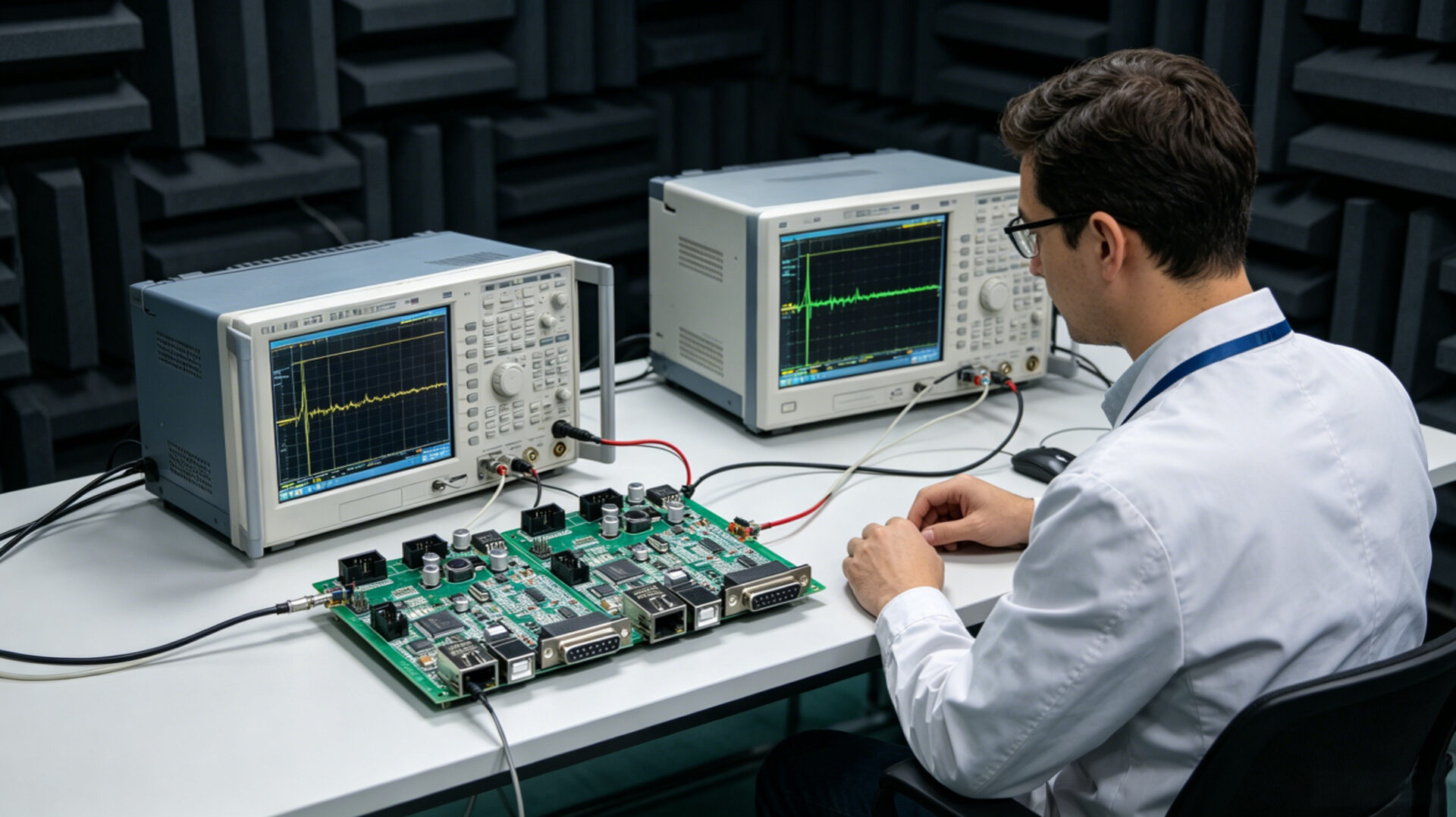
Once the prototype PCBs are assembled, TPS can perform in‑house EMC pre‑compliance testing to validate the design against the target standards—typically CISPR 32 / EN 55032 for conducted and radiated emissions. This is not a full certification test, but it provides high confidence that the design will pass at an accredited laboratory. If emissions are found to exceed limits, the TPS team analyzes the root cause and implements corrective measures—adding snubbers, adjusting gate drive resistors, or modifying the shielding—and re‑tests until the design meets the required limits. This iterative loop, performed before formal certification, saves weeks of schedule delay and thousands in re‑test fees.
5. Documentation and design handover
At the conclusion of the design service, TPS delivers a complete documentation package. This includes the native design files (schematic and PCB layout), manufacturing files (Gerber data, NC drill, pick‑and‑place), a comprehensive BOM with approved alternates, the design calculation notes, and the pre‑compliance test report. This package gives the customer full ownership of the design while providing everything needed to manufacture the board at TPS or at an alternative EMS provider.
6. Application examples: flyback, LLC resonant, and DC‑DC converters
TPS’s custom power supply PCB design service supports the most common topologies in industrial and consumer power conversion:
- AC‑DC flyback converters: For power levels up to approximately 100 W, requiring careful attention to transformer placement, snubber layout, and primary‑secondary isolation.
- LLC resonant converters: For higher‑power, high‑efficiency applications, where the resonant tank layout and gate drive routing are critical to achieving zero‑voltage switching.
- DC‑DC buck and boost converters: For point‑of‑load regulation, battery charging, and distributed power architectures, where input and output capacitor placement directly determines loop stability and EMI.
- Multi‑output and auxiliary supplies: For systems requiring multiple isolated or non‑isolated voltage rails, often with stringent cross‑regulation requirements.
7. RFQ checklist for custom power supply PCB design
- Electrical specification: Input voltage range, output voltage(s) and current(s), total output power, efficiency target, switching frequency preference.
- Isolation requirements: Functional, basic, or reinforced insulation; working voltage and required hipot test voltage.
- Mechanical constraints: Maximum PCB dimensions, height restrictions, preferred connector locations, and mounting hole positions.
- EMC targets: Applicable emission standards (e.g., CISPR 32 Class A or B, EN 55032) and immunity standards (IEC 61000‑4‑x series).
- Production volume: Anticipated annual volume, which influences component selection and design-for-manufacturing decisions.
- Documentation: Required file formats, design reports, and test documentation.
- Additional services: Whether prototyping, assembly, and EMC pre‑compliance testing are required as part of the project.
8. FAQ
Does TPS design the complete power supply, or just the PCB layout?
TPS provides a complete design service from schematic capture through to production‑ready Gerber files. This includes component selection, schematic design, PCB layout, DFM review, and EMC pre‑compliance testing.
What EDA tools does TPS use for PCB design?
TPS uses professional‑grade EDA tools suitable for complex multi‑layer power supply designs. Native design files are provided as part of the final deliverable.
Can TPS design for high‑volume manufacturing?
Yes. DFM is integrated into the design process from day one, ensuring that the layout is optimized for automated SMT assembly, wave soldering, and in‑circuit testing.
Does TPS provide EMC pre‑compliance testing as part of the design service?
Yes, EMC pre‑compliance testing is an integral part of the design validation process, performed in TPS’s own EMC laboratory.
Where can I learn more about TPS’s broader PCB design and assembly capabilities?
Visit the TPS PCB assembly service page, or read our guides on electronic components and assembly and PCB assembly services EMS.