

System integrators and panel builders know that modern electronic systems packing more processing power into smaller enclosures than ever before. A high‑density embedded controller or a sealed industrial IoT gateway generates significant heat from its processors and power converters. While simultaneously being susceptible to—and a source of—electromagnetic interference. When these two physical challenges treated as separate design problems, the result is often a product that passes bench testing but fails thermal cycling or EMC compliance testing, forcing costly, time‑consuming redesigns late in the development cycle.
TPS Elektronik’s thermal and EMC optimized circuit board integration service addresses both challenges simultaneously, within the broader EMS workflow. By considering thermal pathways and electromagnetic compatibility during the PCB assembly and enclosure integration phases, TPS ensures that the finished product operates reliably within its thermal envelope and meets the stringent EMI requirements of its target market.
1. Why thermal and EMC optimization cannot be separated
In a dense electronic enclosure, thermal management and EMC control physically coupled. Adding a heat sink to a power transistor changes the capacitive coupling to the enclosure, which can increase radiated emissions. A conformal coating applied for environmental protection can alter the surface resistivity and affect electrostatic discharge paths. Ignoring these interactions leads to a frustrating cycle where solving a thermal problem creates an EMC problem, and vice versa. TPS’s integrated circuit board integration service, grounded in comprehensive electronic manufacturing capabilities as described in the Electronic Manufacturing Services complete guide, addresses both domains simultaneously. Which ensuring that design decisions in one area do not compromise performance in the other.
2. TPS approach to integrated thermal management
Effective thermal management starts at the PCB assembly stage. During the DFM review for SMD PCB assembly, TPS engineers identify high‑power components and design the thermal pathway. For conduction‑cooled systems, this involves specifying thermal interface materials (TIMs) such as gap pads, phase‑change materials, or thermal grease. And designing a heat spreader that conducts heat to the enclosure wall. For forced‑air systems, TPS models airflow requirements and ensures that component placement and heatsink orientation do not create stagnant hot spots.
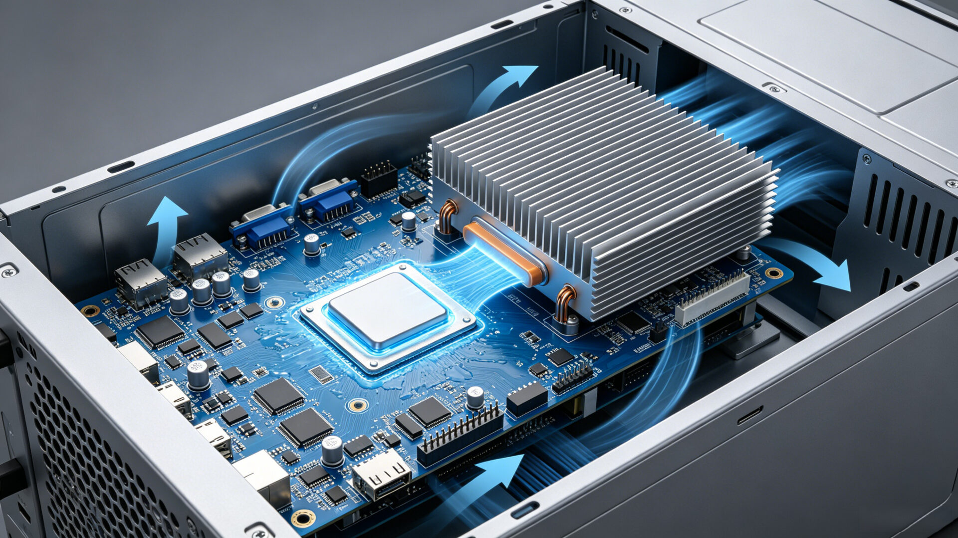
The goal is not simply to add a heatsink, but to create a complete thermal circuit. From the semiconductor junction, through the package, TIM, heat spreader, and ultimately to the ambient environment. That keeps all components below their maximum rated junction temperature. This approach validated through thermal imaging during prototype testing. Which further detailed in our resources on electronic components and PCB assembly testing.
3. TPS approach to board‑level EMC integration
EMC problems most cost‑effectively solved at the board level. TPS’s design review includes an assessment of PCB layer stack‑up, critical signal routing, decoupling capacitor placement, and return path integrity. For sensitive analog or RF sections, TPS can integrate board‑level shielding cans that soldered directly to the PCB. Which providing localized isolation. Where cables exit the board, ferrite beads or common‑mode chokes specified and assembled as part of the integration service.
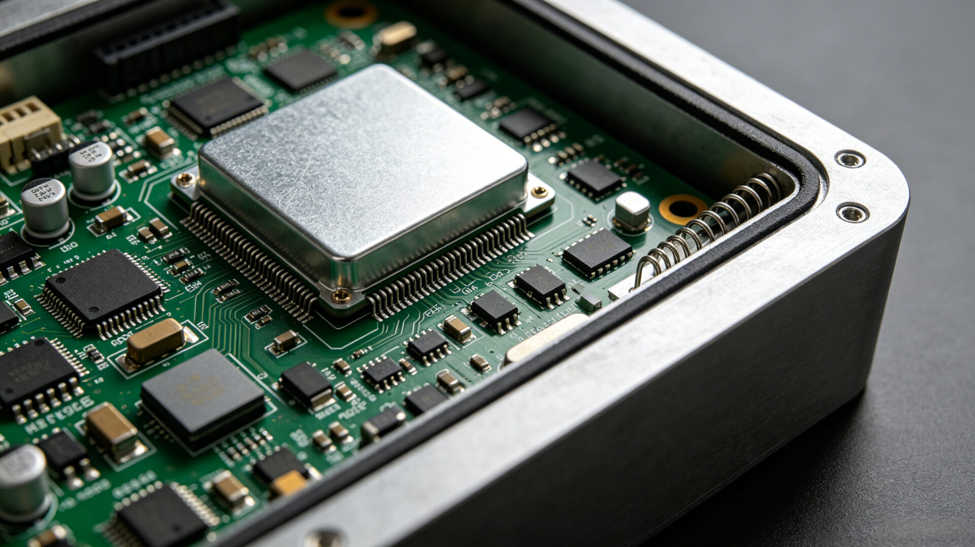
The interface between the PCB and the enclosure is a critical EMC boundary. TPS designs the grounding strategy to ensure a low‑impedance connection between the board’s ground plane and the enclosure at all frequencies of concern. This may involve conductive gaskets, grounding springs, or careful placement of mounting holes. These measures complemented by a rapid prototyping and testing process, similar to what described in our guide on EMS PCB assembly rapid prototyping.
4. The integration process: from PCB to sealed enclosure
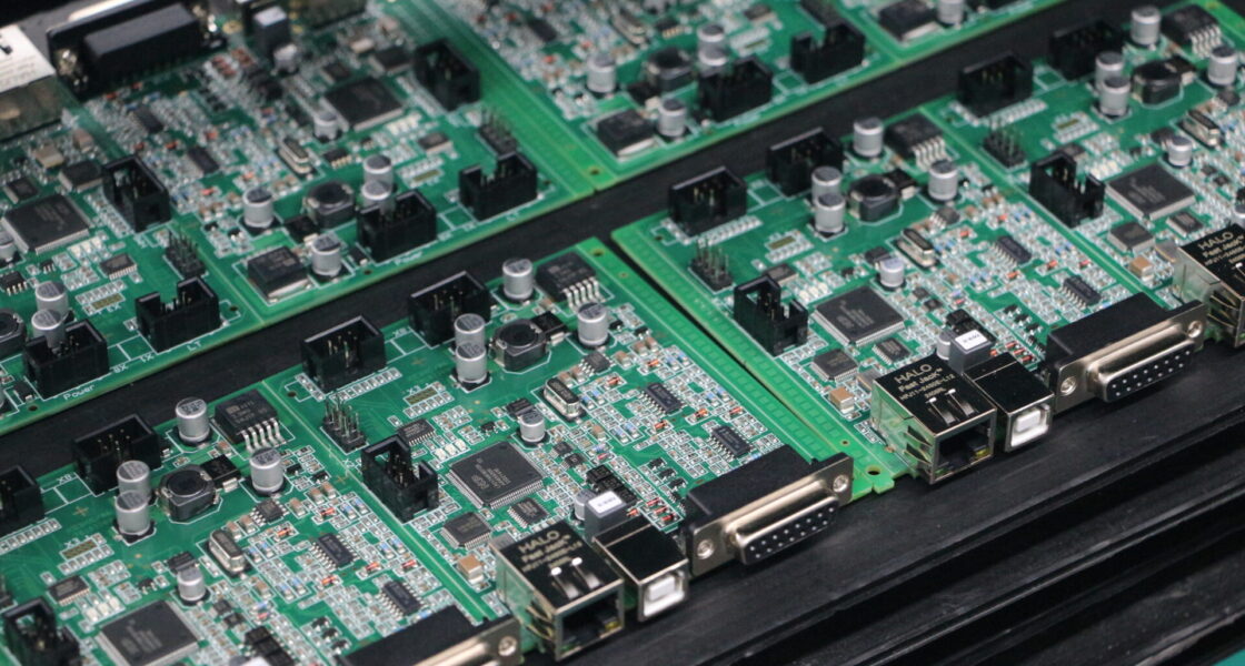
The TPS thermal and EMC optimization service is a fully integrated part of the PCB assembly workflow. After SMT placement, reflow soldering, and inspection, the populated PCB proceeds to system integration. This includes mounting the board into its enclosure, which applying thermal interface materials, installing shielding cans, connecting internal wiring. And applying conformal coating if required for the intended environment. By managing this entire sequence in‑house, TPS eliminates the risk of a third‑party integrator damaging a populated board or compromising the EMC design through improper assembly.
This holistic approach accelerates time‑to‑market by catching integration issues early and ensures that the final assembly meets its thermal and EMC targets. It is an extension of the full EMS offering, which includes everything from component procurement to final testing.
5. Validation: thermal imaging and EMC pre‑compliance
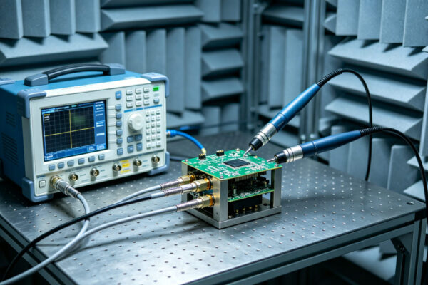
Before a completed assembly leaves the TPS facility, it undergoes validation testing to confirm that the thermal and EMC design targets have been met. A thermal imaging camera used to map the temperature of critical components under full load, verifying that no hot spots exceed design limits. EMC pre‑compliance testing for conducted and radiated emissions can performed in TPS’s own EMC laboratory. Which providing a high degree of confidence that the device will pass formal certification at an accredited test house. This integrated validation process is a core component of delivering reliable, production‑ready electronic systems.
6. Application examples: industrial gateways, medical devices, and automotive telematics
- Sealed industrial IoT gateways: A fanless, sealed enclosure housing a multi‑core processor and a cellular modem requires careful conduction cooling and EMI shielding. TPS’s integration ensures that the processor stays within its thermal limits and that the sensitive receiver not desensitized by onboard digital noise.
- Medical diagnostic devices: Equipment that must meet IEC 60601‑1‑2 EMC immunity standards benefits from TPS’s board‑level shielding and filtered I/O integration, built into the PCB assembly process.
- Automotive telematics units: Compact, ruggedized devices operating in harsh automotive environments demand robust thermal design and immunity to high‑energy transients. TPS’s integration provides the necessary environmental protection and transient suppression.
7. RFQ checklist for thermal and EMC optimized integration
- System description: Enclosure type and material, mounting orientation, and cooling method (conduction, natural convection, or forced air).
- Thermal requirements: Maximum expected ambient temperature, component power dissipation map, maximum junction temperature limits.
- EMC requirements: Target EMI standards (e.g., CISPR 32 Class A/B) and immunity standards (IEC 61000‑4‑x).
- Environmental protection: Required IP rating, conformal coating type, and any special sealing needs.
- Quantities and schedule: Prototype, pilot, and series volumes.
8. FAQ
Does TPS design the thermal solution, or do I need to provide a completed thermal design?
TPS can design the complete thermal solution based on your component specifications and enclosure constraints. Or work from an existing thermal design.
What types of thermal interface materials does TPS work with?
We work with gap pads, phase‑change materials, dispensable thermal greases, and electrically isolating thermal pads, selecting the appropriate material based on thermal conductivity and mechanical gap requirements.
Can TPS perform EMC pre‑compliance testing on the completed assembly?
Yes. Our integrated EMC laboratory can test for conducted and radiated emissions, providing test reports with every project to support your CE marking or FCC submissions.
Where can I learn more about TPS’s broader PCB assembly and integration capabilities?
Visit the TPS PCB assembly service page, or explore our detailed guide on electronic components and testing.