For system integrators, panel builders, and electrical engineers, the journey from a CAD schematic to a functional printed circuit board is fraught with hidden risks. A design that passes software DRC (Design Rule Check) might still be a nightmare to manufacture. When OEMs rush into a fast pcb prototyping service without a thorough manufacturability check, they often face tombstoning components, solder bridges, and obsolete parts—leading to costly revisions and delayed market entry.
This customer case study explores how a leading medical and industrial device manufacturer partnered with TPS Elektronik. By leveraging our free PCB fabrication design review before manufacturing, the client eliminated three critical design flaws, ensuring a flawless first-pass prototype and a seamless transition to mass production.
Request your free DFM review and PCB prototyping quote today →
1. The Challenge: Rushing into PCB prototyping
Our client, an innovative developer of diagnostic monitoring equipment, was on a strict deadline to present a functional prototype to their stakeholders. In the past, they utilized a basic “print-to-order” board house. The previous vendor simply took their Gerber files and manufactured them exactly as drawn, without any manufacturability check PCB protocols.
The result was disastrous. The previous iteration suffered from severe tombstoning on 0402 passive components due to unbalanced thermal mass on the copper pads. Furthermore, two critical ICs specified in the BOM (Bill of Materials) were facing global shortages, halting the assembly process for weeks. The client needed a medical device PCB prototype that was not only fast but guaranteed to be manufacturable and reliable.
They turned to TPS Elektronik, seeking a partner who understood that true PCB design for manufacturing (DFM) happens before the FR4 is ever cut. For more context on our comprehensive approach, see our electronic manufacturing services complete guide.
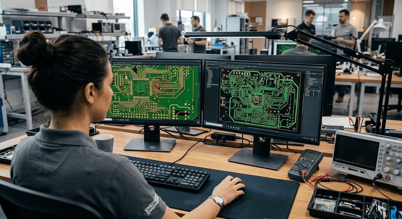
2. The Solution: TPS free DFM analysis PCB prototype review
At TPS Elektronik, we do not just print boards; we engineer solutions. Before initiating our fast pcb prototyping service, our engineering team conducted a comprehensive, free PCB prototype design check. This process aligns with the stringent guidelines set forth by the IPC (Association Connecting Electronics Industries).
2.1 Footprint and thermal relief optimization
During the prototype DFM optimization phase, our CAM engineers identified several critical issues in the client’s layout:
- Acid Traps: Acute angles in the copper traces that could trap etching acid, leading to long-term reliability issues. We smoothed these to 45-degree angles.
- Thermal Reliefs: Several SMT pads were connected directly to massive copper ground planes without thermal reliefs. During reflow soldering, the ground plane would act as a heatsink, causing cold solder joints. We added proper thermal spokes to ensure even heating.
- Solder Mask Expansion: We adjusted the solder mask clearances to prevent solder bridging on fine-pitch QFN packages.
2.2 Proactive PCB prototype component sourcing
A prototype is useless if the parts cannot be procured. Our procurement team conducted a deep dive into the client’s BOM. We identified the two at-risk ICs and immediately proposed pin-to-pin compatible alternatives that were currently in stock. This proactive PCB prototype component sourcing prevented a 12-week delay.
Understanding the nuances of component selection is vital. We detail this process in our guide to electronic components, PCB assembly, and testing.
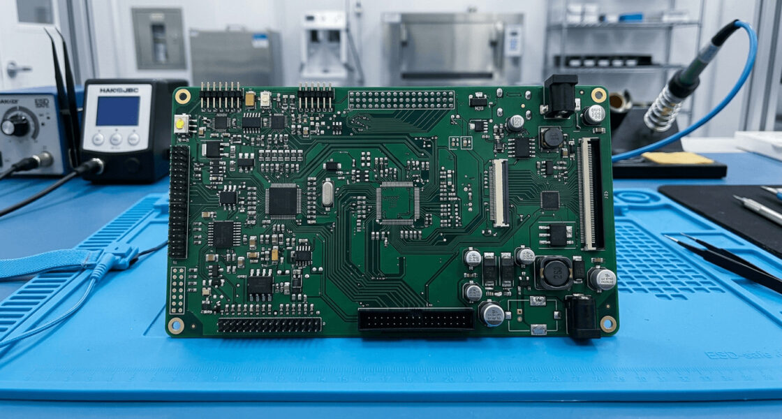
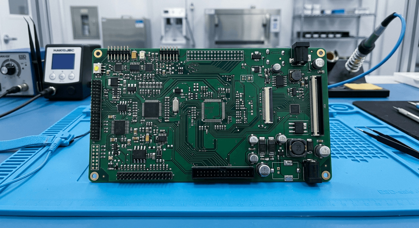
3. The Results: High reliability PCB fabrication on the first run
Because the design was thoroughly vetted, the actual manufacturing process was flawless. The client received their low volume PCB prototype within the expedited timeframe. More importantly, the board functioned perfectly on the first power-up.
By catching the thermal relief and footprint issues during the DFM analysis PCB prototype stage, we saved the client an estimated $4,500 in revision costs and three weeks of engineering rework. The high reliability PCB fabrication ensured that the medical device passed its initial pre-compliance electrical safety tests without any board-level failures.
4. From low volume PCB prototype to turnkey assembly
The ultimate goal of a prototype is to pave the way for mass production. Because TPS Elektronik handled the DFM and the initial build, the transition to series production was seamless. The manufacturing data, optimized solder paste stencils, and validated BOM were already in our system.
The client seamlessly transitioned from a full service PCB prototyping contract to a turnkey PCB assembly prototype and eventually to full-scale production. Whether dealing with complex SMT or robust THT components, our facilities are equipped to scale. Learn more about our capabilities in SMD and THT assembly for industrial manufacturing.
When you partner with TPS, you aren’t just buying a prototype; you are investing in a scalable manufacturing strategy. For medical and high-reliability sectors, this approach is non-negotiable. See our specialized services for medical-grade rapid prototyping.


