System integrators, panel builders, and procurement teams rarely fail because they lack a PCB design. They lose time — and budget. When the assembly partner they selected cannot reliably place 01005 passives, solder 0.5 mm pitch BGAs without voiding, or handle the thermal constraints of a 16‑layer rigid‑flex stack‑up. The result is a prototype that passes bench testing but fails during thermal cycling. Or a pilot build that cannot transition to series production without a complete process requalification.
TPS Elektronik’s PCB assembly service is built to eliminate that gap. From DFM review and component sourcing through SMT placement, X‑ray inspection, conformal coating, and functional test, TPS provides a single accountable source for complex HDI multilayer and rigid‑flex assemblies — documented to IPC‑A‑610 Class 2 or Class 3 and backed by certifications including ISO 9001, ISO 13485, and IATF 16949.
1. Why complex PCB assembly demands more than standard SMT
A standard SMT line that assembles 4‑layer FR‑4 boards with 0603 passives and QFP ICs operates within wide process windows. The same line cannot assemble a 12‑layer HDI board with 01005 components, blind microvias, and 0.4 mm pitch BGAs without fundamental changes to stencil design, solder paste selection, reflow profiling, and inspection methodology. The process window narrows sharply as component density increases.
This is where many PCB assembly services fall short. A provider that markets “BGA capability” may lack the X‑ray inspection necessary to verify hidden solder joints. A provider that claims “rigid‑flex experience” may not have the dedicated carrier fixtures that prevent flex sections from warping during reflow. For system integrators and procurement teams evaluating partners for complex PCB assemblies. These capability gaps translate directly into project risk — manifested as low first‑pass yield, unpredictable lead times, or field failures that erode margins and reputations.
TPS Elektronik addresses this through an integrated EMS approach. The PCB assembly service is not a standalone operation. It embedded within a broader manufacturing infrastructure that includes component sourcing, DFM engineering, mechanical integration, and final system test. For a comprehensive overview of how these services integrate, refer to the Electronic Manufacturing Services complete guide.
2. HDI and multilayer assembly: blind vias, microvias, and thermal management
High‑Density Interconnect (HDI) PCBs defined by finer lines and spaces, smaller vias, and higher connection pad density than conventional PCBs. A typical HDI design uses laser‑drilled microvias (typically 0.1 mm or smaller) to connect outer layers to the next internal layer. Which combined with buried vias for deeper interconnects. These boards demand assembly processes that accommodate reduced pad geometries, tighter solder paste deposition control. And precise reflow profiles that prevent voiding in microvia structures.
TPS addresses HDI assembly through several process controls. Solder paste inspection (SPI) verifies deposit volume and shape on pads that may be as small as 0.2 mm × 0.3 mm. Stencil design for HDI often requires stepped stencils with different thicknesses for fine‑pitch and coarse‑pitch areas on the same board. A capability TPS supports through its stencil procurement and qualification process. Reflow profiles are developed specifically for the thermal mass and layer count of each HDI design. With thermocouple profiling on actual assemblies to validate that all solder joints reach the required peak temperature without exceeding component limits. For additional technical background on PCB assembly processes and component integration, see the electronic components PCB guide.
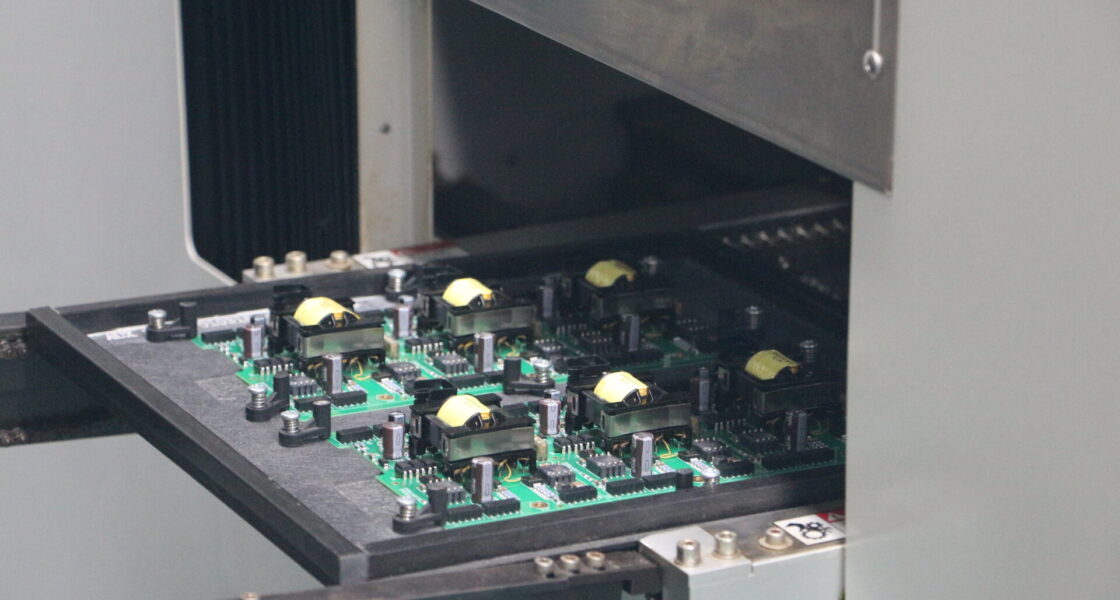
3. Rigid‑flex and flex assembly: fixturing, stiffeners, and reflow control
Rigid‑flex PCBs combine rigid board sections with flexible polyimide circuits in a single structure. This eliminates connectors and cables between sub‑assemblies. Which reducing weight and improving reliability. But it introduces significant assembly challenges. The flexible sections must supported during solder paste printing and component placement to ensure consistent paste deposition and accurate placement. During reflow, the different thermal expansion coefficients of the rigid and flexible materials can cause warping if the board not properly fixtured.
TPS manufactures rigid‑flex assemblies using dedicated carrier fixtures that support the flexible sections throughout the entire SMT process. These fixtures custom‑designed for each board design and ensure that the flex areas remain flat and stationary during paste printing, placement, and reflow. Stiffeners applied where additional mechanical support is needed for connector mounting or high‑stress areas. The process also accounts for the reduced thermal mass of flex sections. With reflow profiles adjusted to prevent overheating of the polyimide substrate while ensuring complete solder wetting on the rigid sections. For an overview of how rigid‑flex and mixed‑technology assembly fits into the broader PCB assembly workflow, refer to the detailed guide on SMD PCB assembly and THT assembly for industrial manufacturing.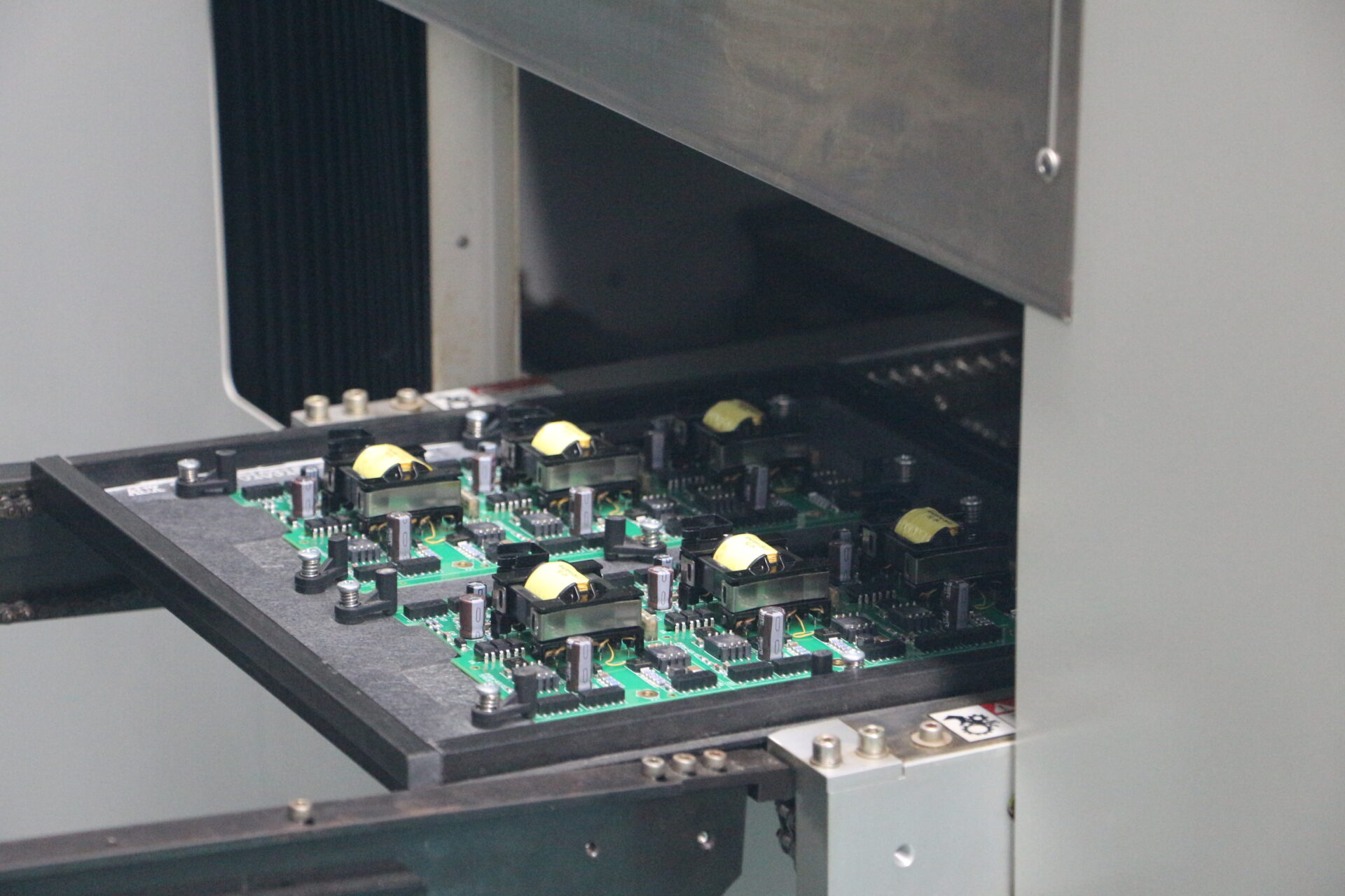
4. BGA and microelectronics capability: µBGA, QFN, and 01005 placement
Ball Grid Array packages concentrate hundreds of connections in a footprint smaller than a postage stamp. A 0.4 mm pitch µBGA with 400 solder balls leaves no room for error: a single bridged or open joint renders the entire assembly non‑functional. QFN packages present a different challenge . Their hidden thermal pad must achieve consistent solder coverage for effective heat transfer. Yet excess voiding beneath the pad degrades thermal performance and can cause device failure under load.
TPS controls BGA and QFN assembly quality through a combination of process and inspection. Solder paste volume is verified by SPI before component placement. Reflow performed in a controlled nitrogen atmosphere to improve wetting and reduce oxidation. After reflow, 3D automated optical inspection (AOI) verifies visible joints, and X‑ray inspection evaluates hidden BGA solder balls for voiding, bridging, and opens. For assemblies requiring the highest reliability, thermal coupons or sacrificial boards used to validate the reflow profile before committing production quantities.
At the opposite end of the size spectrum, 01005 passive components — approximately 0.4 mm × 0.2 mm — require placement accuracy beyond the capability of older pick‑and‑place equipment. TPS’s SMT lines maintain placement capability for these ultra‑small devices, supported by vision alignment and calibrated nozzle systems. For more on BGA process control and inspection protocols, see the EMS PCB assembly: rapid prototyping to medical‑grade production guide.
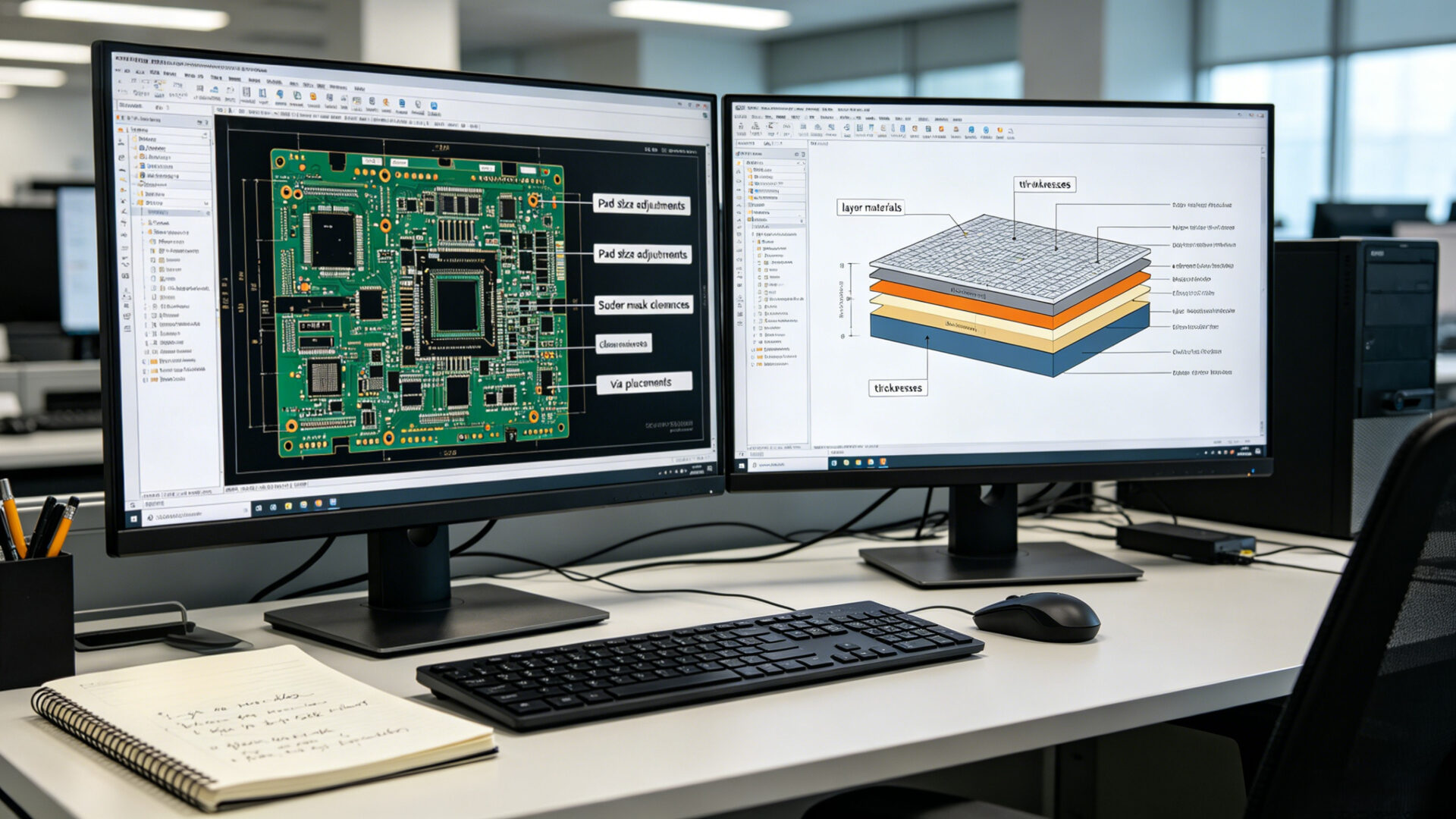
5. DFM integration: catching issues before stencil release
Design for Manufacturability review is the most cost‑effective intervention point in any PCB assembly project. A design that lacks fiducials, specifies insufficient solder mask clearance between fine‑pitch pads, or places tall components too close to the board edge for selective soldering will generate defects on the production line — defects that could have been prevented by a thorough DFM check before Gerber release.
TPS provides DFM feedback as a standard part of every assembly quotation. The engineering team reviews Gerber files, the bill of materials, pick‑and‑place data, and assembly drawings against manufacturing constraints. Typical findings include pad size adjustments for optimal solder joint formation, solder mask dam width verification to prevent bridging. Component‑to‑edge clearance checks for tooling access, and thermal pad via design review for QFN and BGA packages. The DFM report is delivered with the quotation. Which allowing the design team to implement corrections before stencil fabrication begins. For a broader perspective on how DFM integrates into EMS partner selection, refer to the technical guide on PCB assembly services EMS.
6. Quality and testing: AOI, X‑ray, ICT, and functional test
Visual inspection alone cannot verify the integrity of a 400‑ball BGA or detect a tombstoned 0201 capacitor hidden beneath a heat sink. TPS deploys a multi‑stage inspection and test strategy that catches defects at the point of occurrence and verifies functional performance before shipment.
The inspection sequence begins with solder paste inspection (SPI) immediately after printing. Which using 3D measurement to verify paste volume, height, and alignment on every pad. After component placement and reflow, automated optical inspection (AOI) checks component presence, polarity, and solder joint quality on visible connections. For hidden joints — BGA, QFN thermal pads, and press‑fit connectors. X‑ray inspection evaluates solder ball shape, void percentage, and bridging. Electrical test options include in‑circuit test (ICT) with bed‑of‑nails fixtures for high‑volume production. Which flying probe test for prototypes and low‑volume builds, and functional test (FCT) using custom fixtures and software to validate the assembly under simulated operating conditions. All test results are documented in the lot inspection report provided with each shipment.
7. Conformal coating and environmental protection
Electronics deployed in industrial, automotive, or outdoor environments face threats that a bare PCB cannot withstand: moisture ingress, corrosive gases, conductive dust, and fungal growth. Conformal coating — a thin polymeric film applied to the PCB surface. Which protects against these environmental stressors, extending operational life and reducing field return rates.
TPS offers automated selective conformal coating as part of the PCB assembly service. Robotic spray nozzles apply acrylic, silicone, or polyurethane coatings to designated board areas while masking connectors, test points, and components that must remain uncoated. The selective process provides precise edge definition without the manual labor and inconsistency of brush application or the tooling cost of full‑board dip coating. Coating thickness verified by automated measurement, and UV inspection confirms complete coverage of target areas. This capability is particularly relevant for assemblies destined for marine, mining, chemical processing, and outdoor telecommunications environments where humidity and contamination are unavoidable.
8. Certifications and compliance: IPC‑A‑610, J‑STD‑001, and industry standards
For procurement teams evaluating PCB assembly services, certifications provide objective evidence of process capability. TPS Elektronik maintains certifications that are directly relevant to complex electronics manufacturing:
- IPC‑A‑610: The global standard for electronic assembly acceptability. TPS builds to Class 2 (dedicated service) or Class 3 (high performance/harsh environment) acceptance criteria, as specified by the customer. Class 3 assemblies — required for medical, aerospace, and automotive electronics — are produced with documented process controls and inspection records per the IPC‑A‑610F standard.
- J‑STD‑001: The industry standard for soldered electrical and electronic assemblies, defining materials, methods, and verification criteria. TPS soldering processes comply with J‑STD‑001H requirements.
- ISO 9001: Quality management system certification covering all manufacturing and service processes.
- ISO 13485: Medical device quality management system certification, supporting traceability and documentation requirements for FDA and EU MDR submissions.
- IATF 16949: Automotive quality management system certification, supporting PPAP and production part approval requirements.
Compliance with safety standards such as IEC 62368‑1 (the hazard‑based safety standard for AV/ICT equipment) is supported through documented creepage and clearance verification on assembled boards. For a comprehensive overview of the full PCB assembly service scope and certification framework, see the TPS PCB assembly service page.
9. RFQ checklist for complex PCB assembly
To provide an accurate quotation for a complex PCB assembly project, TPS requests the following information:
- Design files: Gerber data (RS‑274X or ODB++), BOM with approved alternates, pick‑and‑place (centroid) file, assembly drawings, and test requirements.
- Board specification: Layer count, board thickness, surface finish (ENIG, HASL, OSP), minimum trace/space, via type (through, blind, buried, microvia), rigid‑flex construction if applicable.
- Component information: Package types on the BOM (BGA, QFN, QFP, 01005, etc.), fine‑pitch components with pitch specification, and any special handling requirements (MSL, ESD sensitivity).
- Quantity and schedule: Prototype quantity, pilot run volume, series production volume, and target delivery dates.
- Acceptance class: IPC‑A‑610 Class 2 or Class 3, including any customer‑specific acceptance criteria.
- Test requirements: ICT, flying probe, functional test specification, X‑ray inspection requirements, environmental stress screening if applicable.
- Conformal coating: Coating type (acrylic, silicone, polyurethane), areas to coat and areas to mask.
- Documentation: Required FAI report, certificate of conformance, material certifications, and PPAP documentation if applicable.
- Sourcing model: Turnkey (TPS procures all components) or consigned (customer supplies components).
10. FAQ
What is the difference between IPC‑A‑610 Class 2 and Class 3?
Class 2 applies to dedicated service electronic products where continued performance and extended life are required, and uninterrupted service is desired but not critical. The Class 3 applies to high‑performance/harsh environment electronic products where continued performance is critical, equipment downtime cannot be tolerated, and the end‑use environment may be uncommonly harsh. Class 3 imposes stricter acceptance criteria for solder joint fill, voiding, and other visual attributes.
Can TPS assemble boards with both SMT and through‑hole components?
Yes. TPS handles mixed‑technology assemblies combining SMT and THT on the same board. The process flow typically completes SMT first (paste print, placement, reflow), followed by through‑hole insertion and selective or wave soldering, with AOI after each soldering stage.
Does TPS support prototype and low‑volume builds as well as series production?
Yes. TPS provides quick‑turn prototyping with DFM feedback, fast stencil procurement, and accelerated programming. The same SMT lines used for production are used for prototypes, ensuring process consistency when transitioning to volume. See the rapid prototyping guide for details.
What file formats does TPS accept for PCB assembly?
TPS accepts Gerber RS‑274X, ODB++, pick‑and‑place (centroid) data in CSV or TXT format, BOM in Excel or CSV, and assembly drawings in PDF. Native CAD files can also be accepted for DFM review.
What certifications does TPS hold for PCB assembly?
TPS is certified to ISO 9001 (quality management), ISO 13485 (medical devices), and IATF 16949 (automotive). Assembly processes comply with IPC‑A‑610 Class 2/3 and J‑STD‑001H soldering standards.
Where can I learn more about TPS PCB assembly capabilities?
Visit the TPS PCB assembly service page, or read the technical guides on PCB assembly services EMS and electronic components and assembly.


