

System integrators, panel builders, and procurement teams in ADAS development rarely lose time because the sensor algorithm is wrong. They lose it when a 77GHz radar board fails its first VNA measurement, when a LiDAR receiver cannot resolve the return pulse because the TIA input sees picofarads of parasitic capacitance, or when an automotive PCB assembly passes functional test but cannot demonstrate the traceability that IATF 16949 and ISO 26262 require.
TPS Elektronik’s development and engineering services, combined with HDI and high-frequency PCBA assembly, built to reduce that risk: stackup and material selection, RF and high-speed layout review, precision assembly of 01005 parts and fine-pitch BGAs. And documentation aligned with automotive quality requirements.
1. Why signal integrity decides radar and LiDAR PCBA success
An ADAS sensor PCBA is not a digital board with a sensor attached. It is an RF or high-speed analog system in which the PCB substrate, the copper geometry, and the assembly quality are part of the signal path. Signal integrity is therefore a board-level property, not a chip-level specification.
1.1 77GHz radar: the board is part of the RF circuit
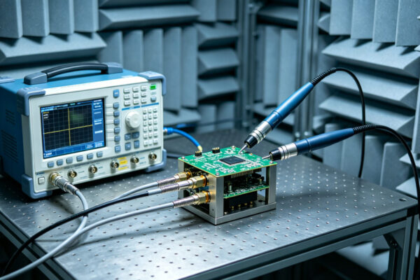
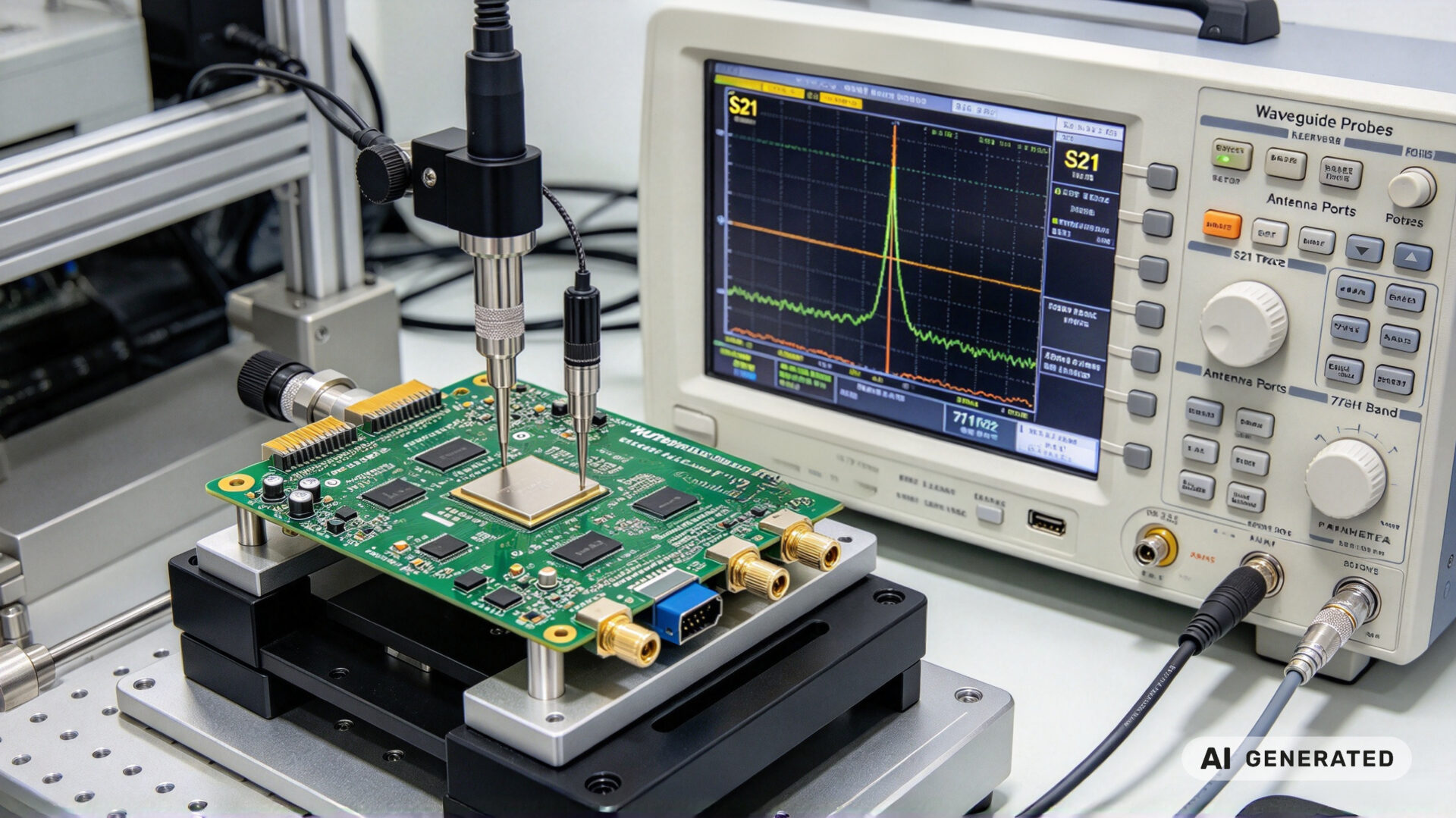
At 77GHz, the guided wavelength on a low-loss laminate is approximately 2.25mm. A 0.1mm trace width error shifts impedance by 3–4Ω. Which is enough to move a quarter-wave matching section away from its simulated length and degrade antenna return loss. Every via stub becomes a resonator, and every discontinuity in the feedline produces a reflection that appears in the VNA measurement as a notch or ripple.
The link budget makes this critical. A 200m long-range radar may have only 2–3dB of total board loss budget; a few centimetres of the wrong material can consume it entirely. The automotive PCB assembly must therefore preserve the dielectric and conductor properties that the RF designer simulated, from the first prototype to the millionth series unit.
1.2 LiDAR: the board is part of the timing circuit
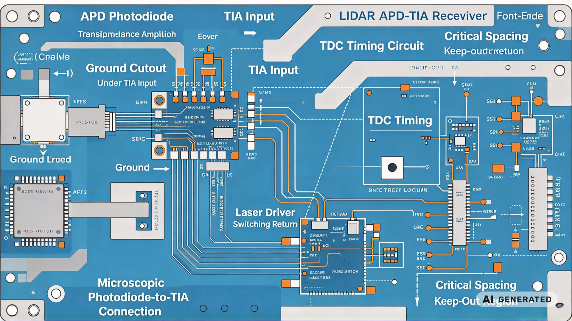
A LiDAR PCBA integrates three functional blocks: a pulsed laser driver, an APD/TIA receiver, and a timing circuit based on a TDC or a high-speed ADC. The receiver’s most sensitive node is the connection between the photodiode and the TIA input. Every picofarad of parasitic capacitance at that node reduces bandwidth and adds noise, directly degrading the time-of-flight resolution.
The second critical constraint is isolation between the transmit and receive domains. The laser driver switches hundreds of milliamps in nanoseconds; its return current must not share copper with the TDC reference or the comparator input, or the switching noise walks straight into the timing measurement.
2. Material and stackup decisions that preserve signal integrity
The substrate is the first and most expensive signal-integrity decision. Choosing it correctly at the concept stage avoids a redesign after the first VNA measurement.
2.1 77GHz radar: low-loss laminates and hybrid stackups
Standard FR-4 has a dissipation factor of roughly 0.020 at 10GHz and becomes unusable above approximately 2GHz for RF signal paths. Rogers RO3003, the de-facto standard for 77GHz automotive radar. Which has a Df of 0.0010 and a Dk of 3.00 ± 0.04, stable across 10–110GHz. Rogers RO4830 Plus is a newer woven-glass-free thermoset laminate with a design Dk of approximately 3.03 at 77GHz and an insertion loss of 1.5dB/inch for 5mil laminates, positioned for cost-sensitive 76–81GHz corner radar.
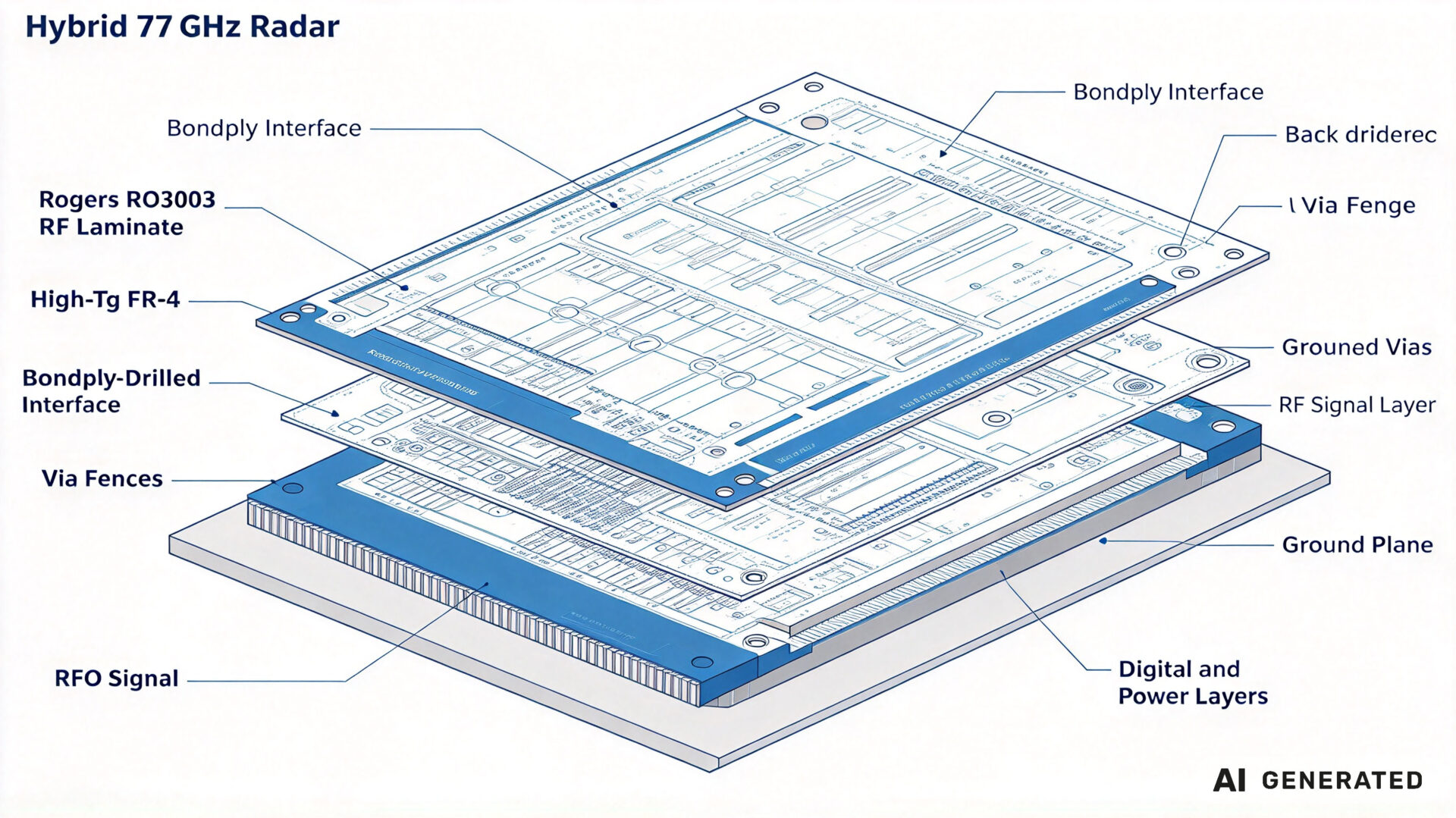
A pure RO3003 build is unnecessarily expensive for a production radar module. The practical approach is a hybrid stackup: low-loss RF laminate on the top one or two layers for the antenna array and feedlines, bonded to high-Tg FR-4 for the inner digital and power layers. This reduces material cost by 30–50% versus an all-Rogers build without compromising antenna performance. The bondply and the plated-through via transition between the two materials must be simulated, because the via stub and the material transition are both impedance discontinuities.
2.2 LiDAR: mixed-signal partitioning and high-speed interconnect
LiDAR boards mixed-signal by nature: a nanosecond, high-current laser driver on one side, a single-photon-sensitive receiver on the other. The material choice is usually a high-Tg FR-4 or a low-loss digital laminate, because the critical issue is not millimetre-wave loss but return-path integrity and crosstalk between the driver and the TIA.
The stackup must provide an uninterrupted reference plane under the TIA input and under the high-speed digital links (LVDS or Ethernet). The APD bias supply should be treated as part of the signal chain: APD gain rises exponentially with bias, so bias noise multiplies directly into the received signal. A dedicated, filtered bias layer or a local LDO close to the APD is often necessary.
3. Layout rules that make the difference
Material selection sets the ceiling; layout determines whether the design reaches it. The rules below are the ones that most often separate a first-pass success from a respin.
3.1 Radar RF layout: impedance, via fences, and back-drilling
Route all RF traces as microstrip or stripline with field-solver-verified dimensions. At 77GHz, the tolerance on trace width and dielectric thickness is tight enough that calculator tables are insufficient when Dk varies with temperature and lot. Surround antenna arrays and RF feedlines with via fences at 0.5–1.0mm pitch, tying all ground planes together; via fences suppress surface waves that corrupt the antenna radiation pattern.
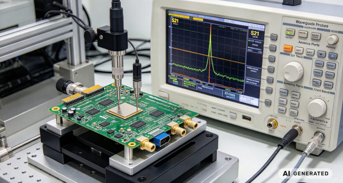
Back-drill all plated-through vias in the RF signal path. An undrilled stub resonates at a fraction of the wavelength at 77GHz and produces standing waves in the feedline, visible as sharp notches in the VNA S21 trace. Use immersion silver (ImAg) on the RF layers: at 77GHz the skin depth in copper is approximately 0.24µm, and ENIG’s nickel barrier sits in the current path and adds conductor loss.
Separate the RF section from digital and power circuitry with a physical gap of at least 5mm, bridged only by a continuous stitching-via row. A single switching regulator within coupling distance of the antenna can push radiated emissions above CISPR 25 Class 5 limits.
3.2 LiDAR receiver layout: the microscopic connection
Keep the photodiode-to-TIA connection as short as physically possible. Every picofarad at that node costs bandwidth. A ground cutout under the TIA input pin reduces parasitic capacitance to the surrounding copper. This is a standard layout technique for high-speed transimpedance amplifiers.
Physically separate the TDC or comparator reference from the laser driver’s switching return. The driver’s current loop and the timing circuit’s reference must not share a return path, or the switching transient appears as timing jitter. If the board includes a high-speed ADC instead of a TDC, treat its clock and reference pins with the same discipline as an RF feedline: controlled impedance, uninterrupted reference plane, and distance from the driver.
4. How TPS HDI and high-frequency assembly supports the design
TPS Elektronik provides development and engineering services alongside HDI and high-frequency PCBA assembly. The capability relevant to radar and LiDAR is the combination of layout engineering, material and stackup selection. And precision assembly under automotive quality documentation.
4.1 DFM review and simulation-led stackup
TPS’s development team works with Altium Designer and Cadence Allegro for schematic capture and PCB layout, and reviews the stackup and material selection against the RF and high-speed requirements before release. For radar boards, this includes the hybrid RF/FR-4 interface, via transitions, and back-drill requirements. For LiDAR boards, it includes the APD-TIA node, the TDC reference plane, and the driver return path.
4.2 Precision assembly and inspection
Radar and LiDAR PCBAs use fine-pitch BGAs, QFNs, and 01005 passives alongside the RF front-end. TPS’s HDI assembly line supports 12-layer HDI boards with 01005 components, blind microvias, and 0.4mm pitch BGAs, with SPI, AOI, and X-ray inspection for hidden solder joints. Conformal coating is available where the module requires environmental protection.
4.3 Automotive traceability and documentation
Automotive radar and LiDAR PCBAs fall under IATF 16949 for the production process and AEC-Q100/Q200 for the components. ISO 26262 adds functional-safety traceability, with ASIL B requiring SPFM ≥90% and LFM ≥60% at the hardware level. TPS’s documentation package supports this by providing assembly records, material declarations, inspection results, and traceability data that the Tier 1 or OEM can reference in the PPAP and functional-safety evidence package.
The TPS HDI PCBA service page describes the process scope, and the custom power supply and buck-boost converter design resources cover related power-integrity work for the sensor’s supply rails.
5. RFQ checklist for radar and LiDAR PCBA
To streamline quotation and engineering review for an automotive pcb assembly with RF or LiDAR signal-integrity requirements, provide the following information:
- Board type and function: 77GHz radar front-end, LiDAR receiver/driver, camera module, or sensor-fusion ECU
- RF or high-speed specifications: Operating frequency, impedance targets (50Ω single-ended / 100Ω differential), insertion-loss budget, and data rate
- Material and stackup: Proposed RF laminate (e.g., RO3003, RO4830 Plus, RO4350B), hybrid construction, layer count, and copper weight
- Critical layout features: Antenna array, via fences, back-drilled vias, APD-TIA node, TDC reference, and driver return path
- Assembly requirements: Component types (01005, fine-pitch BGA, QFN), inspection scope (SPI, AOI, X-ray), conformal coating
- Automotive standards: IATF 16949, AEC-Q100/Q200, ISO 26262 ASIL level, and the required PPAP documentation
- Test requirements: VNA S-parameter measurement, functional test, and any thermal or reliability screening
- Volume and schedule: Prototype, pilot, and series quantities with delivery milestones
Providing these details reduces clarification cycles. TPS’s engineering team can support material selection, stackup definition, and layout review as part of the RFQ process.