System integrators and panel builders rarely see the mechanical drawings that dictate whether a high‑density electronic enclosure will function as intended. A semiconductor test equipment manufacturer learned this lesson when their latest‑generation instrument failed thermal validation. Not because of a circuit design flaw, but because the custom aluminum heat sink and copper I/O panel were machined with insufficient flatness. The resulting 50‑micron gap between the heat sink and the power transistors caused a 12 °C junction temperature rise. Which pushing the device outside its safe operating area.
TPS Elektronik’s precision CNC milling service was brought in to solve the problem. The goal: achieve 5‑micron flatness and positional tolerances across multiple aluminum and copper parts. And integrate the mechanical deliverables with the instrument’s PCB assembly and final test. All under one quality system.
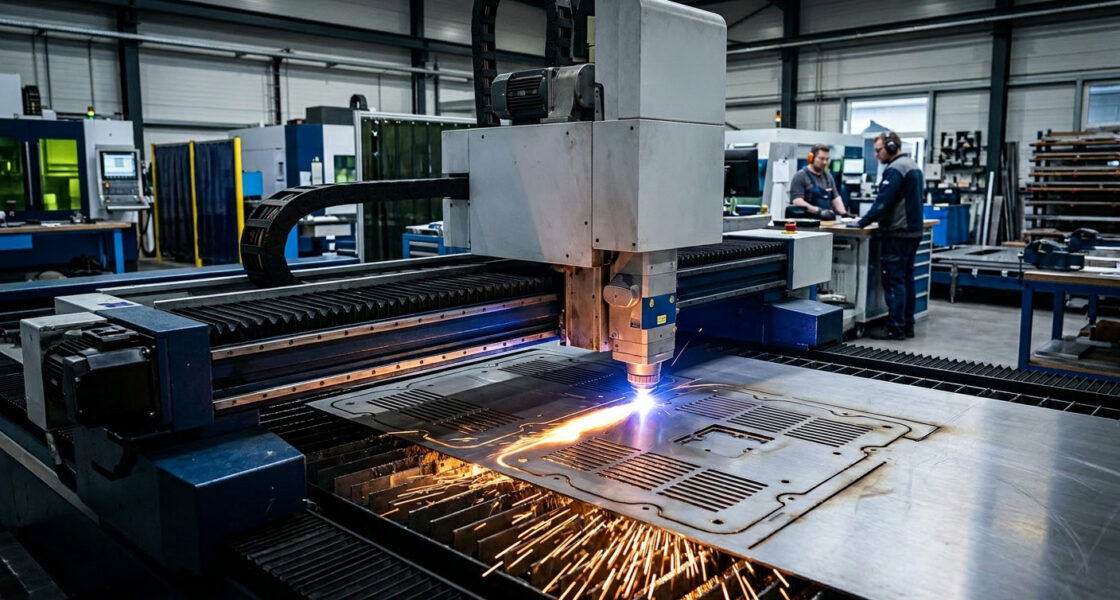
1. The machining challenge: 5‑micron tolerances in aluminum and copper
The test instrument contained two critical machined components: an aluminum heat sink with precision‑milled fin channels and mounting bosses. And a copper I/O panel that formed part of the RF shielding enclosure. The heat sink required flatness of 5 µm across the transistor mounting surface to ensure uniform thermal interface material (TIM) compression. The copper panel needed positional tolerances of ±5 µm on the connector cutouts, because any deviation would misalign the SMA connectors with the PCB‑mounted jacks. Which creating impedance discontinuities in the RF path.
Aluminum and copper present opposite machining challenges. Aluminum 6061‑T6 is relatively soft and can gall if cutting speeds and coolant delivery are not optimized. Copper is ductile and abrasive, causing rapid tool wear if the wrong carbide grade or coating is selected. Achieving 5‑micron tolerances in both materials on the same production line demands precise control of spindle speed, feed rate, tool runout, and thermal growth of the machine itself.
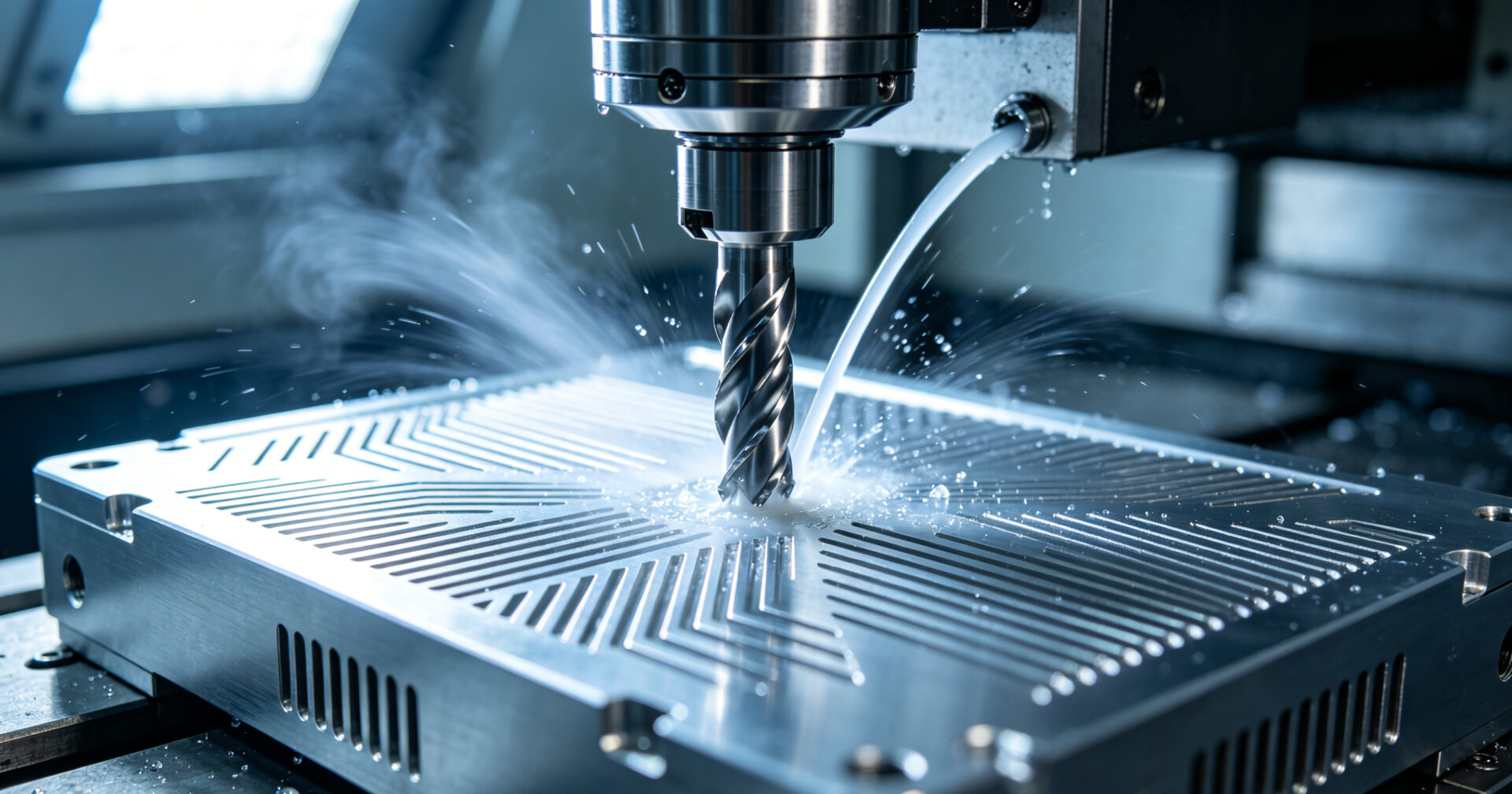
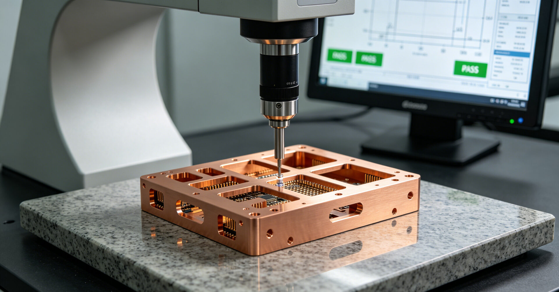
TPS addressed these challenges through a combination of high‑speed machining centers equipped with thermal compensation, balanced tool holders with runout below 3 µm. And in‑process probing that verified critical dimensions between operations. The aluminum heat sink machined with polished carbide end mills and high‑pressure coolant to prevent chip re‑cutting. The copper panel machined with diamond‑coated tools to extend tool life and maintain edge quality. Both components inspected on a coordinate measuring machine (CMM) with a volumetric accuracy of 1.5 µm, against a CAD‑based datum system that matched the PCB assembly reference points. For further detail on precision machining capabilities, refer to the TPS guide on precision CNC machining for high accuracy.
2. DFM integration: closing the gap between PCB and enclosure
A common failure mode in outsourced machining is the disconnect between the mechanical drawing and the PCB assembly. A machinist can deliver a part that meets every dimension on the drawing and still produce an enclosure that does not fit the PCB, because the drawing datums chosen independently from the board outline and connector positions.
TPS eliminated this risk through an integrated DFM review. The enclosure CAD model overlaid with the PCB assembly data, and critical interfaces — mounting hole patterns, connector cutouts, thermal pad contact areas — were checked for alignment and tolerance accumulation. One issue identified early was that the original design specified a 2.0 mm wall thickness at the SMA connector cutouts, which left insufficient material for secure connector fastening after plating. TPS recommended increasing the local thickness to 2.5 mm, a change that would have required a complete redesign if discovered after machining. For a broader perspective on integrating design with machining, see our article on EMS CNC milling for electronics: RFQ, DFM, and fixture strategy.
3. Measurable results: flatness, fit, and thermal performance
The outcome of the TPS precision CNC milling intervention validated through three measurable criteria. First, CMM inspection of the aluminum heat sink confirmed a flatness of 4.3 µm across the transistor mounting surface. Which exceeding the 5 µm requirement. Second, the copper I/O panel and aluminum enclosure body assembled to the PCB without any rework. All 24 SMA connector positions aligned within the positional tolerance, confirmed by a go/no‑go fixture. Third, the thermal validation test showed a junction‑to‑ambient thermal resistance (RthJA) within 3 % of the simulated value. Which confirming that the TIM bond line thickness was uniform and the heat sink performed as designed.
From a procurement perspective, consolidating precision machining with the existing EMS partnership reduced the supplier count and eliminated the need for incoming dimensional inspection. A cost that the customer had previously absorbed through a dedicated metrology technician. Full dimensional reports and material certificates provided with each delivery lot, supporting the customer’s ISO 9001 documentation requirements. For more detail on scaling from prototype to production with consistent quality, refer to our guide on EMS CNC milling: high‑precision machining from prototype to production.
4. RFQ checklist for precision enclosure machining
- CAD models and drawings: 3D STEP or IGES files with GD&T annotations for all critical features. Native files accepted.
- Material specification: Alloy and temper (e.g., AL6061‑T6, Cu‑ETP), plating or surface treatment requirements.
- Tolerance requirements: Target flatness, positional, and profile tolerances. Indicate which features are critical‑to‑function.
- PCB interface data: Board outline, connector positions, and mounting hole locations for alignment verification.
- Quantities and schedule: Prototype, pilot, and series volumes with target delivery dates.
- Inspection and documentation: Required dimensional reports, material certificates, and any customer‑specific FAI or PPAP formats.
5. FAQ
What tolerances can TPS achieve in aluminum and copper CNC milling?
TPS routinely achieves tolerances of ±5 µm for critical features such as flatness, positional accuracy, and profile tolerances. Achievable tolerance depends on part geometry, material, and feature size.
How does TPS ensure that machined enclosures fit the PCB assembly?
We perform an integrated DFM review overlaying the enclosure CAD model with the PCB assembly data. Critical interfaces — mounting holes, connector cutouts, thermal contact areas — are checked for alignment and tolerance accumulation before machining begins.
What inspection documentation is provided?
Full CMM dimensional reports traceable to calibrated instruments are delivered with each production lot. Material certificates, FAI reports per AS9102, and PPAP documentation can be provided upon request.
Can TPS machine both prototype and production quantities?
Yes. Prototypes are machined on the same equipment and with the same process documentation used for series production, ensuring a seamless transition from prototype to volume without requalification.
Where can I learn more about TPS CNC milling capabilities?
Visit the TPS CNC milling service page or read our technical overviews on types of milling machines and top CNC milling machine options.


