

System integrators and OEMs rarely fail because they lack a power conversion concept. They lose time—and budget—when the physical power supply circuit board cannot handle the thermal and current density required to meet aggressive size targets. A global manufacturer of high‑power industrial laser systems faced this exact barrier when developing a next‑generation laser driver. Their existing power supply design, built on a standard 2‑ounce copper PCB, was overheating and could not be shrunk into the smaller enclosure demanded by the market. The project risked a major delay.
TPS Elektronik’s custom power supply circuit board design and heavy copper PCB assembly service eliminated this bottleneck. By re‑engineering the board with a 6‑layer, 6‑ounce copper construction, an optimized thermal layout, and embedded press‑fit power terminals, TPS delivered a power supply that met the ultra‑high power density target while passing full EMC and thermal validation. This case study describes the collaboration and the manufacturing techniques that made it possible.
1. The power density challenge
The laser OEM needed a 2.5 kW power supply to fit into a 4U rack chassis, a 40 % volume reduction from the previous generation. The standard FR‑4 PCB with 70 µm copper could not carry the peak currents of 120 A without excessive voltage drop and heating. Thermal imaging showed hot spots exceeding 120 °C on the output inductor pads, degrading efficiency and threatening long‑term reliability. The procurement team urgently needed a partner who could deliver a customized power supply circuit board with integrated, high‑current density design, without compromising safety compliance per IEC 62368‑1. This challenge aligns with the complex manufacturing integration discussed in the Electronic Manufacturing Services complete guide.
2. TPS custom PCB design and heavy copper solution
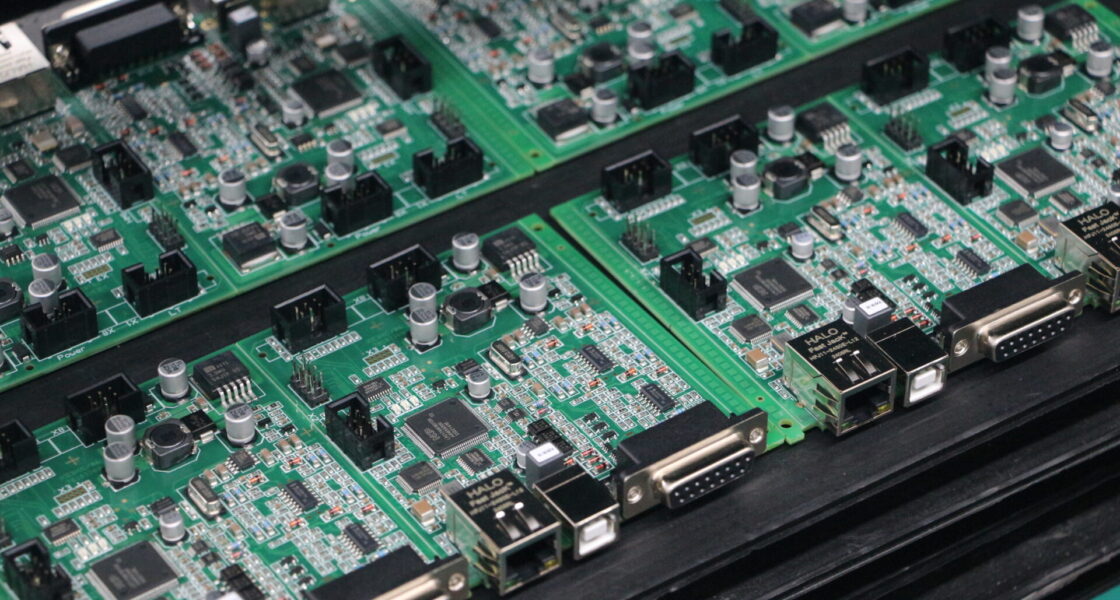
TPS proposed a complete redesign of the power supply board, leveraging its integrated design‑for‑manufacturing (DFM) expertise and heavy copper processing capabilities. The approach focused on a 6‑layer board with 175 µm (6 oz) copper on the outer layers and 105 µm (3 oz) on the inner layers, combined with a thermally optimized component placement. The complete process is detailed in our overview of SMD PCB assembly and THT assembly.
2.1 PCB stack‑up and thermal management
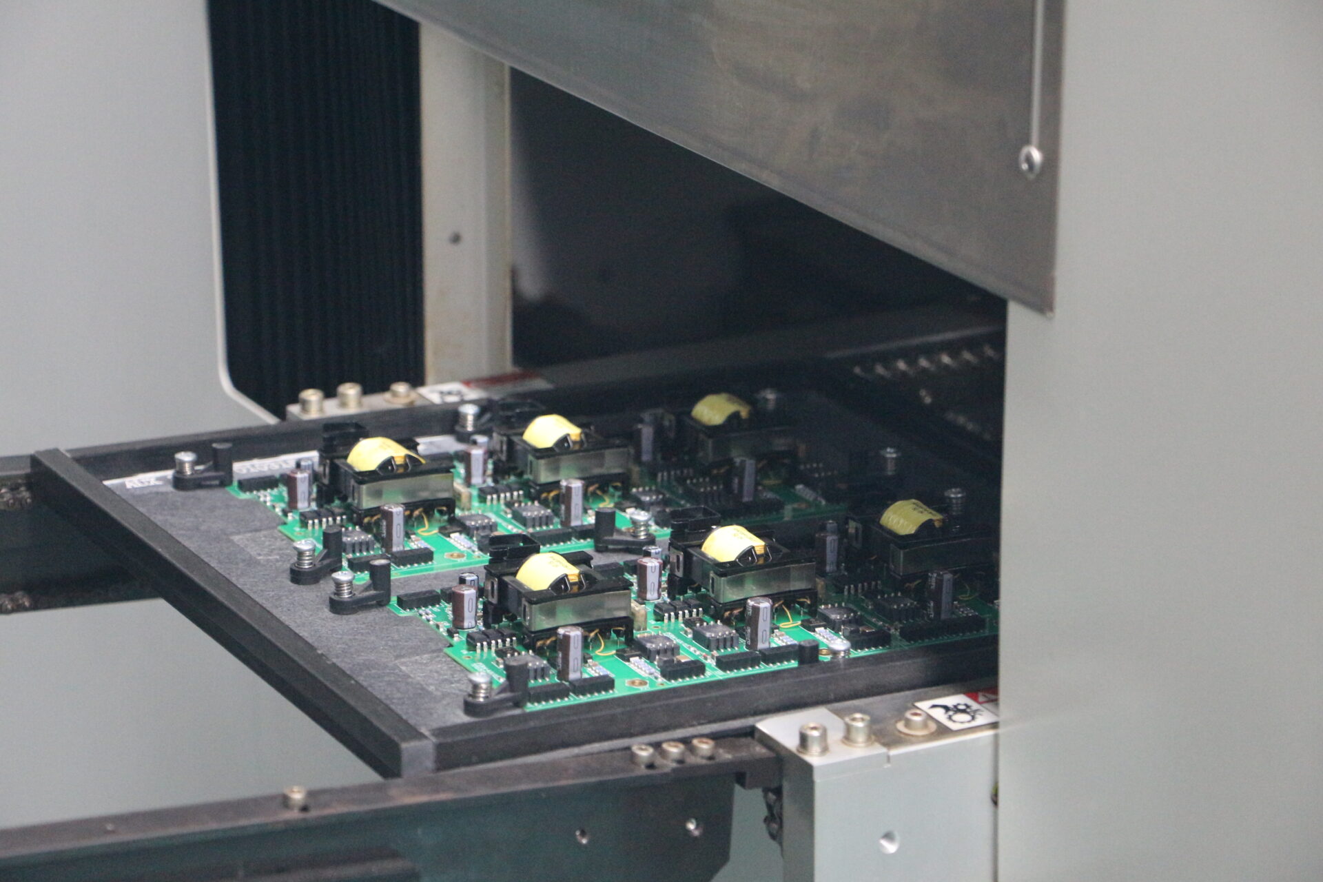
The new stack‑up placed thick copper pours directly under the GaN power transistors and planar transformer, using an array of thermal vias to conduct heat to a large copper area on the bottom layer, which acted as an integrated heat spreader. This passive cooling strategy eliminated the need for a dedicated heatsink, saving precious millimeters of height. TPS engineers also simulated the current density and thermal profile during the design phase, as referenced in the electronic components PCB guide, ensuring that no trace exceeded a 20 °C temperature rise at full load.
2.2 Heavy copper assembly and press‑fit technology
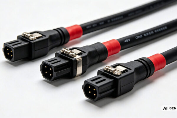
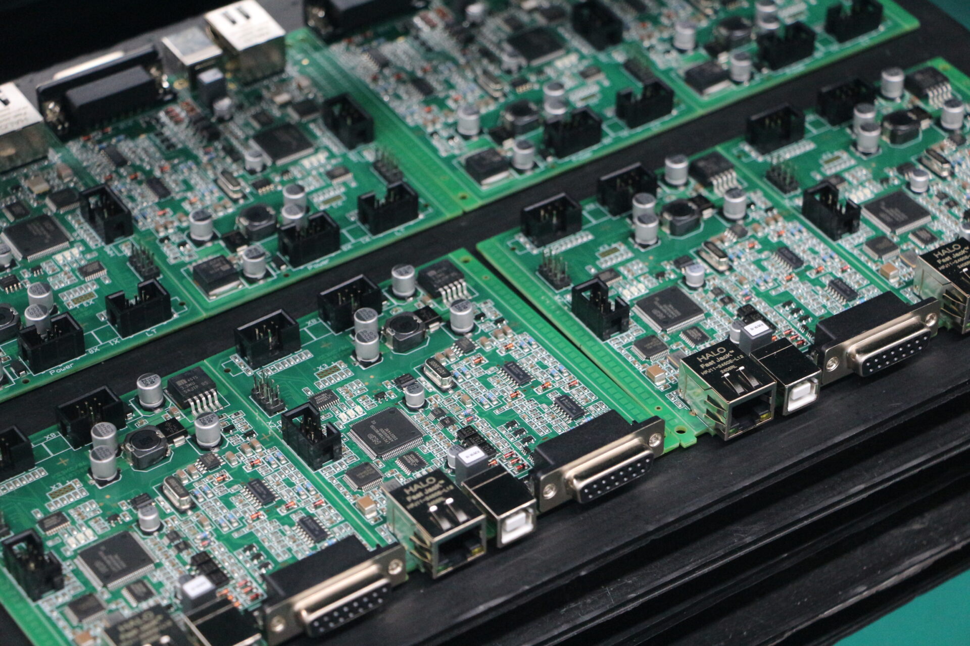
Assembling thick copper boards presents unique challenges. The high thermal mass of heavy copper requires a carefully controlled reflow profile to achieve proper solder wetting without overheating sensitive components. TPS adjusted its SMT process to deliver a robust solder joint on the massive power planes. For high‑current interconnects, TPS integrated press‑fit power terminals directly into the PCB, eliminating the need for hand‑soldered cables. This not only improved reliability but also streamlined the final box‑build integration, a service detailed in our EMS PCB assembly rapid prototyping guide.
3. Measurable results: power density and reliability
The final power supply board met all design goals. The power density reached 110 W per cubic inch. Thermal imaging confirmed that hot spot temperatures remained below 85 °C in a 40 °C ambient, a 35 °C reduction from the previous design, with no airflow required. The press‑fit terminals handled 120 A continuously with a contact resistance of less than 50 µΩ. The integrated, custom PCB assembly passed conducted emissions testing on the first attempt, enabling the OEM to launch the new laser system on schedule. This success highlights the importance of combining advanced PCB design with heavy copper assembly for achieving next‑generation power density targets.
4. RFQ checklist for high‑density power supply PCBs
- Power requirements: Output power, voltage, and peak current per rail.
- Mechanical constraints: Maximum board dimensions and height restrictions.
- Copper weight: Preferred outer and inner layer copper thickness.
- Thermal management: Available cooling method (convection, conduction, forced air).
- Certifications: Applicable safety standards (e.g., IEC 62368‑1).
- Production volume: Prototype and series quantities.
5. FAQ
What is the thickest copper TPS can process on a power supply PCB?
TPS routinely processes outer layer copper weights up to 210 µm (6 oz), and can handle heavier copper for specific high‑current applications upon request.
How does heavy copper help achieve higher power density?
Thicker copper significantly reduces resistive losses and allows the PCB to act as its own heat sink, eliminating separate heat spreaders and enabling more compact designs.
Can TPS combine heavy copper with press‑fit connectors?
Yes, TPS has extensive experience integrating press‑fit power terminals into heavy copper boards, providing a reliable, high‑current interconnect without soldering.
Where can I learn more about TPS’s PCB design and assembly capabilities?
Visit the TPS PCB assembly service page or read our overview of electronic manufacturing services.