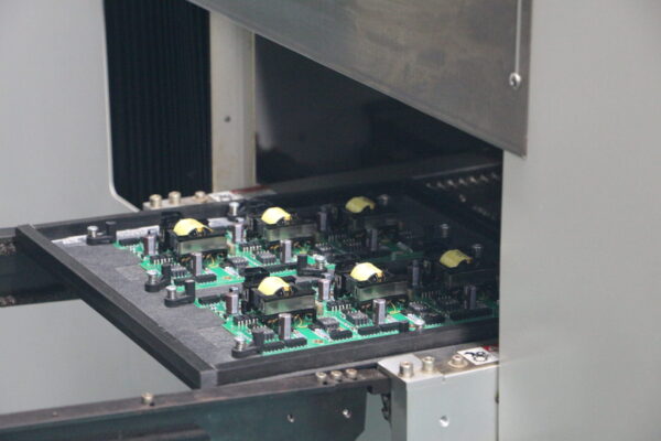


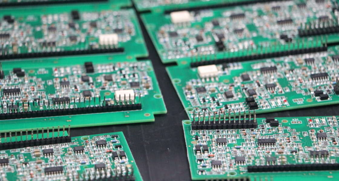
For system integrators, panel builders, and procurement teams developing next-generation electronics, the assembly of ultra-fine pitch and high-density BGA components is not a routine process—it is a precision manufacturing challenge that separates capable EMS partners from those who cannot deliver. A 0.4 mm pitch µBGA with 400 solder balls leaves no room for error. One misaligned placement, one void in a hidden solder joint, or one thermal excursion during reflow can render an entire high-value assembly unusable.
TPS Elektronik’s SMT assembly services are built to meet this challenge: advanced pick-and-place equipment for ultra-fine pitch components, controlled reflow profiling for void-free BGA soldering, and comprehensive inspection including 3D AOI and X-ray for hidden joint verification. From DFM review through series production, TPS delivers high-density PCB assemblies documented to IPC-A-610 Class 2 or Class 3 and backed by ISO 9001, ISO 13485, and IATF 16949 certifications.
1. The BGA Assembly Challenge: Why Standard SMT Lines Fall Short
A standard SMT line that assembles 4-layer FR-4 boards with 0603 passives and QFP ICs operates within wide process windows. The same line cannot assemble a 12-layer HDI board with 01005 components, blind microvias, and 0.4 mm pitch BGAs without fundamental changes to stencil design, solder paste selection, reflow profiling, and inspection methodology. The process window narrows sharply as component density increases.
This is where many PCB assembly services fall short. A provider that markets “BGA capability” may lack the X-ray inspection necessary to verify hidden solder joints. A provider that claims “rigid-flex experience” may not have the dedicated carrier fixtures that prevent flex sections from warping during reflow. For system integrators and procurement teams evaluating partners for complex PCB assemblies, these capability gaps translate directly into project risk—manifested as low first-pass yield, unpredictable lead times, or field failures that erode margins and reputations.
TPS Elektronik addresses this through an integrated EMS approach. The PCB assembly service is embedded within a broader manufacturing infrastructure that includes component sourcing, DFM engineering, mechanical integration, and final system test. For high density BGA assembly and fine pitch PCB assembly applications, this integration ensures that every aspect of the assembly process is controlled and documented.
2. Advanced Equipment for Ultra-Fine Pitch and Micro-Component Assembly
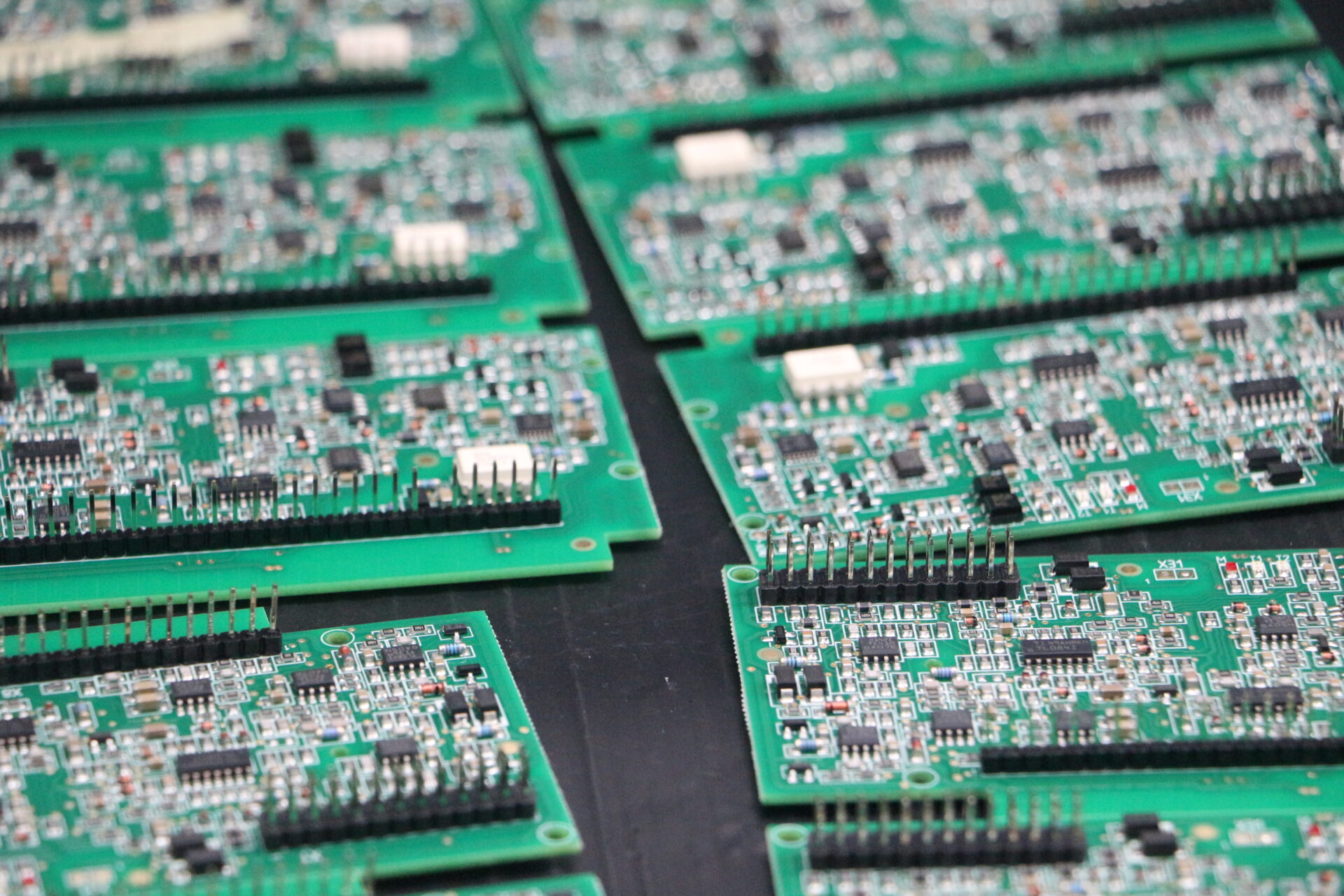
High-density PCB assembly demands equipment that can place components with exceptional precision while maintaining high throughput. TPS Elektronik’s SMT lines feature high-speed pick-and-place machines capable of handling ultra-fine pitch components down to 01005 metric. This ensures perfect solder joints for complex components like BGAs and QFNs, which are critical for high-density PCB assembly.
Key equipment capabilities for advanced SMT assembly include:
- High-speed placement: Modern automated assembly can reach up to ~80,000 components per hour with placement accuracy around ±25 µm, depending on equipment, design, and process setup
- Vision systems: Advanced component alignment cameras ensure precise placement of ultra-fine pitch BGAs with minimal offset
- Multi-zone reflow ovens: Profiled for exact thermal management of complex thermal profiles required for HDI and BGA assemblies
- 3D solder paste inspection (SPI): Verifies deposit volume and shape on pads that may be as small as 0.2 mm × 0.3 mm
For micro BGA PCB assembly applications, the combination of high-accuracy placement and precise process control ensures that even the smallest components are placed correctly and soldered reliably. TPS supports both lead-free (RoHS/REACH) and leaded soldering profiles, with documented traceability and clear build reports.
3. Process Control: Stencil Design, Paste Printing, and Reflow Profiling
High-density BGA assembly requires meticulous process control at every stage of the SMT line. TPS Elektronik’s approach to advanced SMT assembly services includes rigorous control of stencil design, solder paste printing, and reflow profiling.
Stencil Design for HDI and Fine-Pitch Components:
Stencil design for HDI often requires stepped stencils with different thicknesses for fine-pitch and coarse-pitch areas on the same board. TPS supports this through its stencil procurement and qualification process, ensuring that aperture ratios and printing parameters are optimized for each specific PCB design. Typical squeegee force is calibrated between 22–67 N (5–15 lbf) for consistent paste deposition.
Solder Paste Inspection (SPI):
TPS uses 3D SPI to verify solder paste volume and shape on every pad before component placement. This is particularly critical for fine-pitch BGA pads where paste volume variation can lead to opens, bridges, or voiding. TPS controls the BGA and QFN assembly quality through a combination of process control and inspection.
Reflow Profiling:
BGA components require controlled reflow atmospheres and precise thermal profiling. TPS develops and validates reflow profiles for each assembly, using thermal coupons for profile verification where required. Fine-pitch, uBGA/CSP/QFN, and 01005 passives are processed with cavity-reduced reflow profiles to minimize voiding and ensure reliable solder joint formation.
4. Inspection and Quality: 3D AOI and X-Ray for Hidden Joints
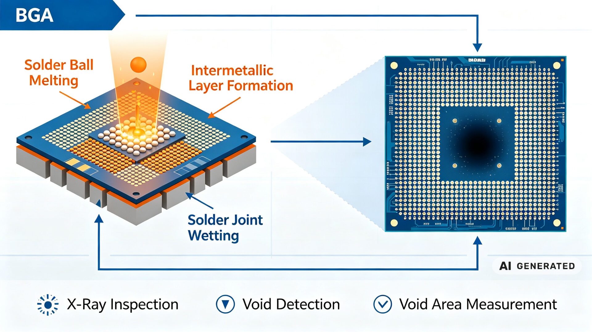
BGA components present a unique inspection challenge: the solder joints are hidden beneath the component body, making them invisible to standard optical inspection. TPS Elektronik addresses this with 3D AOI and X-ray inspection for BGAs and BTCs.
3D Automated Optical Inspection (AOI):
3D AOI inspects visible aspects of the assembly, including component placement accuracy, solder joint shape, and surface defects. For fine-pitch components, 3D AOI provides the resolution needed to detect subtle defects that 2D inspection would miss.
X-Ray Inspection:
X-ray inspection is essential for verifying hidden solder joints beneath BGAs, QFNs, and other bottom-terminated components. TPS uses X-ray to detect:
- Solder voids: Voids in BGA solder joints that can compromise mechanical and electrical reliability
- Bridging: Unintended solder connections between adjacent balls
- Insufficient solder: Joints with inadequate solder volume
- Misalignment: Components that are not properly centered on their pads
Typical measures for BGA process control include paste volume management, controlled reflow atmosphere, X-ray inspection for hidden joints, and use of thermal coupons for profile verification. Such controls are particularly important in regulated sectors such as medical and automotive electronics.
For BGA rework and assembly applications, TPS also offers rework and repair services including NPI bring-up, ECO implementation, BGA reball/rework, and lifecycle support for OEM programs.
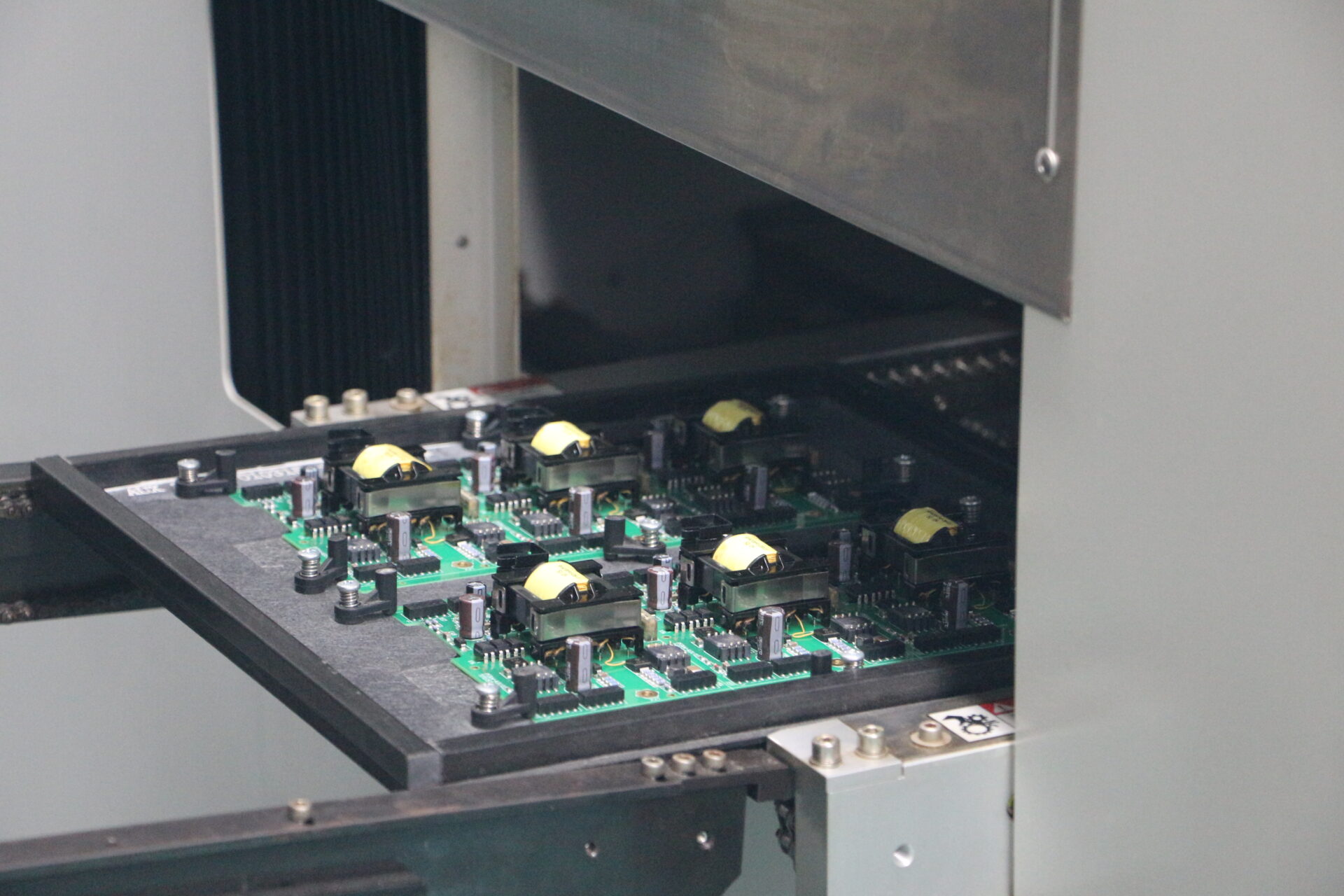
5. Micro-Component Capability: 01005 and Beyond
High-density PCB assemblies increasingly rely on micro-components to achieve the required functionality within constrained board space. 01005 metric passives are among the smallest standard components available—measuring just 0.4 mm × 0.2 mm—and they present significant handling and placement challenges.
TPS Elektronik’s high density SMT assembly capability includes reliable placement of 01005 passives, QFN components, and uBGA/CSP packages. Key considerations for micro-component assembly include:
- Stencil design: Optimized aperture ratios for consistent paste deposition on tiny pads
- Pick-and-place programming: Specialized placement parameters to handle small, lightweight components without misalignment
- Reflow profiling: Cavity-reduced profiles that minimize voiding and prevent tombstoning
- Inspection: 3D AOI with sufficient resolution to verify placement and solder joint quality
For microelectronics SMT assembly applications, the ability to reliably place 01005 and other micro-components is a key differentiator. TPS’s high-speed pick-and-place machines are capable of handling ultra-fine pitch components down to 01005 metric, ensuring perfect solder joints for complex components like BGAs and QFNs.
6. TPS Advanced SMT Assembly Capabilities
TPS Elektronik’s SMT assembly services for ultra-fine pitch and high-density BGA components combine advanced equipment, process control, and comprehensive quality assurance in a single integrated workflow.
Assembly Capabilities:
- Surface-Mount (SMT): Fine-pitch, uBGA/CSP/QFN, 01005 passives with cavity-reduced reflow profiles
- Through-Hole (THT): Selective, wave, or controlled hand soldering with dedicated fixtures and AOI
- Mixed & Special Processes: Rigid-flex and flex, press-fit, shields, heatsinks, LED optics, magnetics integration
- Box build integration: Thermal management and final system assembly
Engineering Support:
- DFM/DFA feedback: Early-stage design review to optimize for manufacturability and testability
- Prototyping & NPI: Fast stencils, quick kitting, clear build notes; EVT bring-up and rework support
- Turnkey procurement: Full or partial turnkey: BOM sourcing, incoming QC, manufacturing, and logistics
Quality and Testing:
- 3D AOI & X-ray for BGAs/BTC: Comprehensive inspection of visible and hidden solder joints
- ICT, flying-probe, boundary-scan, FCT: In-circuit and functional testing with firmware flash
- IPC-A-610 Class 2/3 compliance: Documented to the highest workmanship standards
- Serialization & MES links: Full traceability and quality documentation
- Ionic cleanliness checks: Verification of board cleanliness for reliability
Certifications:
- ISO 9001: Quality management systems
- ISO 13485: Medical device quality management
- IATF 16949: Automotive quality management
TPS supports projects from rapid prototyping through high-volume series production, with documented processes that ensure repeatability and traceability at every stage. For high density interconnect assembly and advanced PCB assembly technology applications, TPS provides the capability, quality, and documentation that complex electronics projects demand.