

For system integrators, electrical engineers, and procurement teams in the optical networking industry, the transition from NRZ to PAM4 signaling at 56Gbps per lane is not a simple upgrade—it is a fundamental shift in PCB material selection, impedance control, and assembly precision. A 56Gbps PAM4 signal has an eye height that is one-third that of NRZ, making it exquisitely sensitive to dielectric loss, impedance discontinuities, and manufacturing variations.
TPS Elektronik’s high frequency PCB assembly service for 56Gbps PAM4 optical modules is built to address these challenges: ultra-low loss material assembly with Panasonic Megtron 6, precision microstrip impedance control, and rigorous signal integrity validation—from prototype to volume production.
1. The 56Gbps PAM4 Signal Integrity Challenge
The explosive growth in AI cluster interconnect bandwidth is creating an entirely new class of PCB substrate requirements. 400G and 800G optical transceivers—in QSFP-DD, OSFP, and CFP8 form factors—rely on 56Gbps PAM4 signaling to achieve the required data rates. At these speeds, signal integrity is not a design afterthought; it is the primary constraint that determines whether a module will pass bit error rate (BER) targets.
PAM4 (Pulse Amplitude Modulation with 4 levels) encodes two bits per symbol, doubling the data rate compared to NRZ at the same Nyquist frequency. A 56Gbps PAM4 signal has a unit interval (UI) of approximately 35.7 ps. The signal amplitude (eye height) of a PAM4 signal is one-third that of an NRZ signal. This means that the signal-to-noise ratio is reduced by 33% (9.5 dB), exacerbating the effects of loss, crosstalk, and jitter. Every picosecond of skew, every 0.1 dB of additional loss, and every impedance discontinuity directly degrades the eye opening and increases BER.
For high speed optical module PCB applications, the challenges are compounded by the dense form factor of QSFP-DD and OSFP modules. The PCB must accommodate high-speed differential pairs, power distribution, and control signals—all within a limited footprint. The routing from the connector to the optical engine and DSP must maintain controlled impedance across the entire channel while minimizing crosstalk and insertion loss. A standard FR-4 board running at 56 Gbps PAM4 will lose 1.0–1.5 dB/inch on inner-layer striplines, exhausting most transceiver equalization budgets before the signal reaches the receiver.
2. Ultra-Low Loss Material Selection: Why Megtron 6
Material selection is the single most important decision for 56Gbps PAM4 PCB design. The dielectric loss (dissipation factor, Df) determines how much signal energy is absorbed by the PCB material per unit length. For 56Gbps PAM4 channels, the Nyquist frequency is 28 GHz. At these frequencies, even small differences in Df translate to significant differences in insertion loss.
Panasonic Megtron 6 has emerged as the industry-standard material for 56Gbps PAM4 applications. Key electrical properties include:
- Dielectric constant (Dk): Approximately 3.4–3.7 depending on glass style and resin content
- Dissipation factor (Df): 0.004 at 10 GHz, with variants achieving 0.002–0.0029 at higher frequencies
- Data rate support: 28–56 Gbps PAM4, with sub-8-inch 112G channels possible
Megtron 6 is built on a modified polyphenylene ether (PPE) resin system, which provides significantly lower loss than standard FR-4 or even mid-loss materials like FR408HR. The material’s transmission loss is close to that of PTFE resin. For 56G PAM4 channels under 12 inches, Megtron 6 remains fully viable.
For ultra-low loss material assembly, TPS works with Megtron 6 (R-5775 series) with verified material properties and controlled impedance on critical pairs. TPS can also implement mixed-dielectric stackups—placing Megtron 6 on high-speed signal layers while using high-Tg FR-4 on power, ground, and low-speed layers. This approach saves 55–65% on the material bill compared to a full Megtron build, while holding channel performance where it matters.
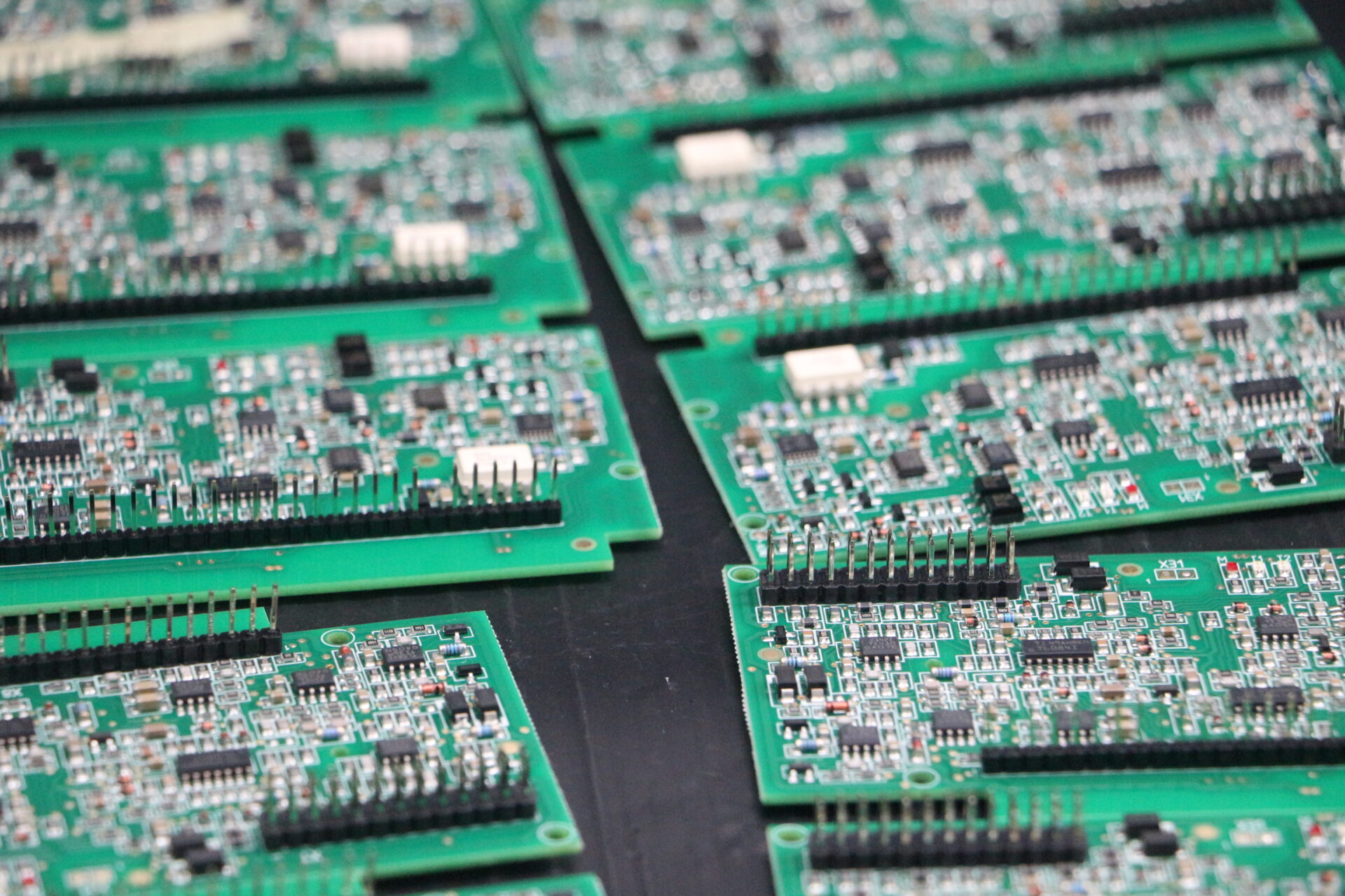
For high frequency PCB assembly service applications, the combination of Megtron 6 and precision assembly ensures that the PCB material does not become the limiting factor in the link budget.
3. Microstrip Impedance Control for Optical Module PCBs
In 400G and 800G optical modules, the high-speed signals from the QSFP-DD or OSFP connector must travel to the optical engine and DSP with minimal signal degradation. The choice of transmission line structure—microstrip vs. stripline—has a direct impact on signal integrity, loss, and manufacturability.
Microstrip traces are on the outer layers of the PCB, with a single reference plane below. For 56Gbps PAM4 optical modules, microstrip is often the preferred choice for short breakout routing from the QSFP-DD connector because:
- Lower dielectric loss: The effective Dk of microstrip is ~60–70% of the laminate Dk because the field is partially in air
- Easier probing and debugging: Outer-layer traces are accessible for measurement
- Shorter via transitions: Reduced via stub length minimizes reflections
However, microstrip has trade-offs: higher radiation loss, susceptibility to surface roughness effects, and sensitivity to soldermask (which increases effective Dk by 0.3–0.5).
For signal integrity RF PCB applications at 56Gbps, the microstrip design must account for:
- Trace width and dielectric thickness: The impedance is fundamentally a ratio of height-to-width scaled by dielectric properties
- Copper roughness: A hidden variable that affects conductor loss at high frequencies
- Differential pair coupling: Tighter coupling reduces differential impedance; typical targets are 85Ω or 100Ω
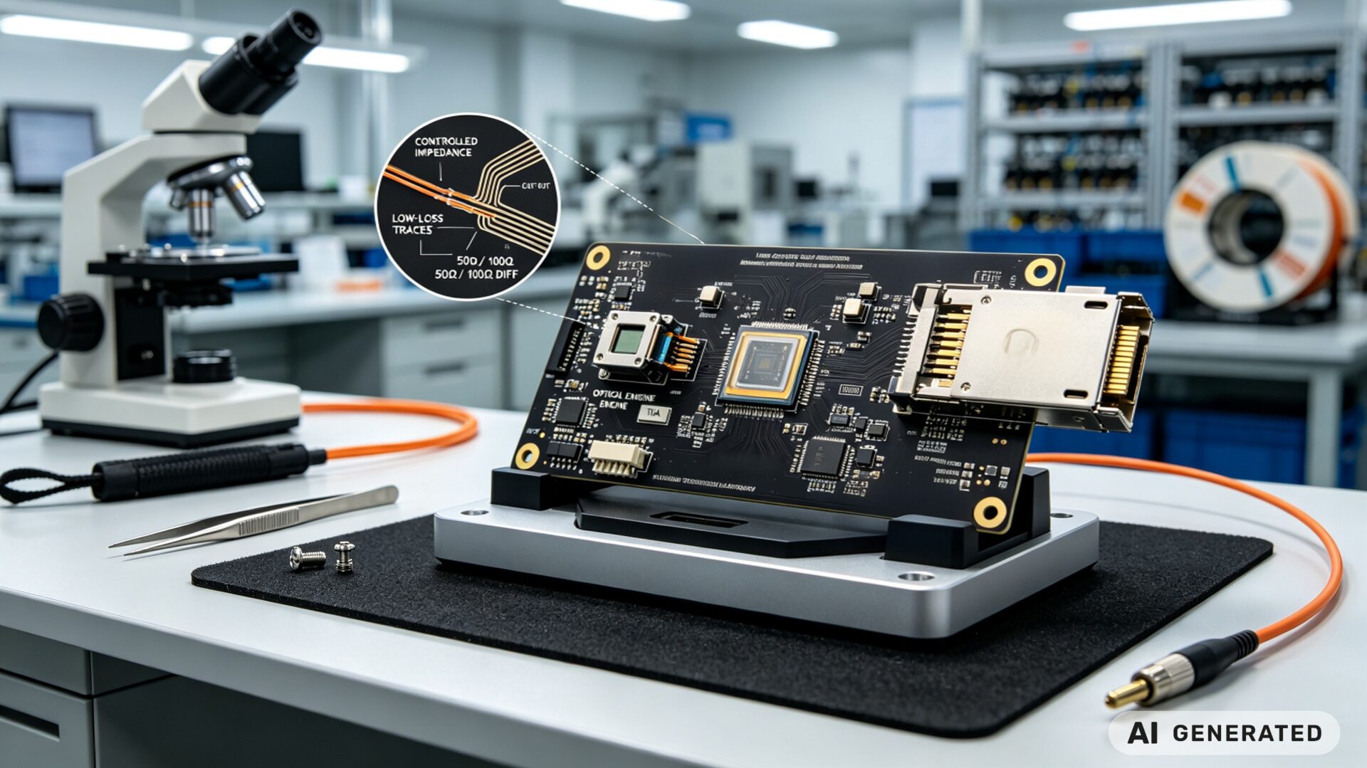
For transceiver impedance control assembly, TPS uses controlled impedance manufacturing with tight tolerances—typically ±10% for impedance, and ±3 mils for trace width on premium 56G PAM4 designs. This precision is essential for achieving the target 100Ω differential impedance with the 5-6 mil trace widths typical of 56Gbps PAM4 designs.
4. Stackup Design and Controlled Impedance
Controlled impedance stackup design is the foundation of 56Gbps PAM4 signal integrity. Get impedance wrong, and the design suffers reflections, ringing, eye diagram degradation, and bit errors. Get it right, and 56 Gbps PAM4 channels work on the first spin.
For 56Gbps PAM4 PCB assembly, the stackup design must consider:
- Reference plane continuity: Every signal trace must have a continuous, unbroken reference plane on an immediately adjacent layer
- Dielectric thickness tolerance: Specify ±0.5 mil or better
- Dk tolerance: Low-loss laminates with Dk tolerance ±0.05
- Via optimization: Designing vias to have accurate input impedance matching all the way up to 56 GHz
- Back-drilling: Removes unused via stubs that cause reflections
For optical module flex-rigid PCB applications, the stackup must also accommodate the transition between rigid and flexible sections while maintaining impedance control across the flex bend region—a significant challenge for 56Gbps signals.
TPS Elektronik’s high speed optical module PCB assembly service includes stackup design guidance, impedance simulation, and manufacturing verification to ensure that the as-built impedance matches the design target. TPS works with customers to define the stackup, material selection, and impedance targets before manufacturing begins.
For data center optical interconnect PCB applications, the combination of controlled impedance, low-loss materials, and precision assembly ensures that the link budget is maintained across the entire channel—from the QSFP-DD connector through the PCB traces to the optical engine.
5. Assembly Precision for High Frequency PCBs
For 56Gbps PAM4 optical modules, PCB assembly precision is as critical as the PCB fabrication itself. At 28 GHz Nyquist frequency, even small assembly variations can degrade signal integrity.
Key assembly considerations for high frequency PCB assembly service:
- Component placement accuracy: ±0.05mm placement precision for BGA and QFN components
- Solder joint consistency: Controlled solder paste volume and reflow profile to minimize impedance variations at component interfaces
- Via and pad optimization: Anti-pad design to reduce via capacitance and maintain impedance
- Surface finish selection: ENIG, ENEPIG, or immersion silver—each with different RF performance characteristics
- Cleanliness: Removal of flux and contaminants that can affect high-frequency performance at 28 GHz and beyond
The copper foil used in the PCB also matters. Megtron 6 uses high-frequency ultra-low profile (H-VLP) copper foil, which minimizes conductor loss. During assembly, the surface preparation and soldering processes must preserve the integrity of the copper surface to maintain consistent RF performance.
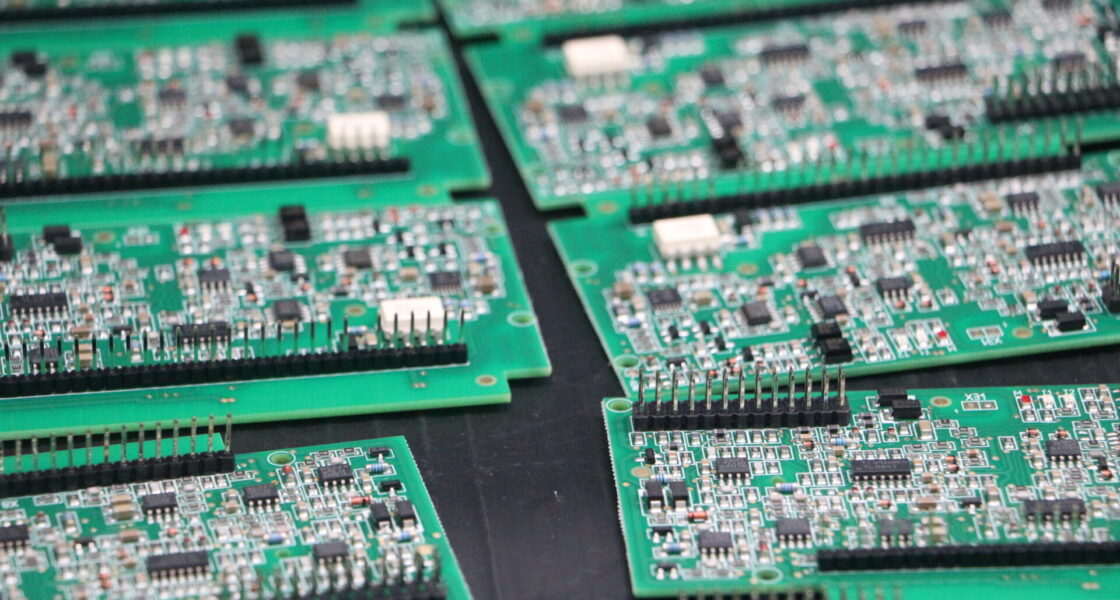
For 400G optical transceiver PCB assembly, the DSP and optical engine components are typically fine-pitch BGAs with high I/O counts. The assembly process must accommodate these components while maintaining the signal integrity of the high-speed lanes. TPS uses advanced SMT assembly equipment with vision inspection and X-ray inspection to verify component placement and solder joint quality.
6. TPS High Frequency PCB Assembly Capabilities
TPS Elektronik’s high frequency PCB assembly service for 56Gbps PAM4 optical modules combines material expertise, precision manufacturing, and signal integrity validation in a single integrated workflow.
Material and Stackup Engineering:
- Megtron 6 (R-5775 series) assembly with verified material properties
- Mixed-dielectric stackups—Megtron 6 on high-speed layers, high-Tg FR-4 elsewhere
- Controlled impedance design with ±10% tolerance (premium ±3% available on critical pairs)
- Dk/Df characterization and material verification
PCB Assembly Capabilities:
- Fine-pitch BGA and QFN placement for DSP and optical engine components
- Controlled reflow profiling for low-loss laminate compatibility
- X-ray inspection for BGA solder joint verification
- Surface finish options: ENIG, ENEPIG, immersion silver, immersion tin
- Cleanroom assembly for optical component handling
Signal Integrity Validation:
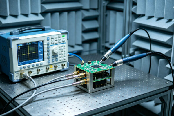
- Time-domain reflectometry (TDR) impedance measurement
- Vector Network Analyzer (VNA) S-parameter measurements up to 50 GHz+
- Eye diagram analysis for PAM4 signal validation
- Insertion loss and return loss verification
- BER testing for complete transceiver validation
Quality and Compliance:
- ISO 9001 and IATF 16949 quality management
- IPC-6012E Class 3 and IPC/WHMA-A-620 workmanship
- First Article Inspection (FAI) with comprehensive reports
- Full material traceability and Certificates of Conformance
TPS supports both prototype and production volumes, with scalable manufacturing capacity for optical module programs of any size. TPS’s high frequency PCB assembly service is integrated with broader EMS capabilities—including optical component sourcing, module assembly, and system integration—reducing supply chain complexity for system integrators and procurement teams.