

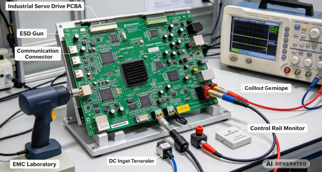
System integrators, panel builders, and procurement teams in motion control rarely lose time because the servo algorithm is wrong. They lose it when a drive resets during an ESD event at the encoder connector, when a surge on the 24V auxiliary rail destroys the interface transceiver, or when the unit passes functional test on the bench and fails immunity at the accredited lab—forcing a PCBA redesign, a new layout spin, and a delayed machine launch.
TPS Elektronik’s industrial control PCBA services built to reduce that risk: protection-stage integration at the connector, ground partitioning reviewed before layout release. And EMC-oriented assembly and inspection from prototype through series production.
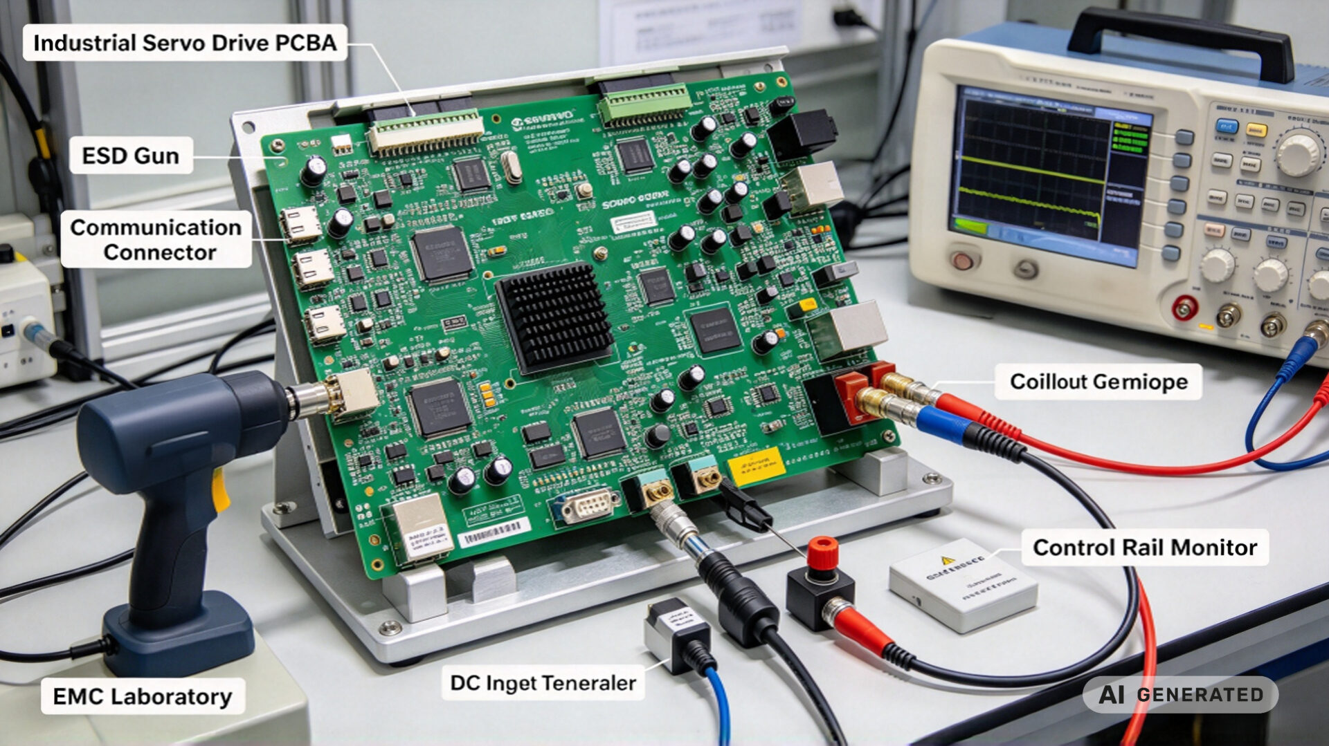
1. What ±4kV surge and ±15kV ESD actually mean for a servo drive PCBA
The numbers ±4kV and ±15kV are not arbitrary. They come from the basic immunity standards that the servo drive product standard references. And they applied to specific ports of the drive, not to the PCBA as a whole.
1.1 IEC 61000-4-2 ESD: contact vs. air discharge
IEC 61000-4-2 defines four test levels. Level 4 corresponds to 8kV contact discharge and 15kV air discharge. In servo drive practice. Which contact discharge is applied to accessible conductive parts—connector shells, mounting screws, chassis—while air discharge is applied to insulated surfaces and slots. A servo drive specification of “±15kV” typically refers to the air-discharge level, with contact discharge at a lower but still severe level (often ±4kV or ±8kV) depending on the accessible metal.
The waveform is the human-body model: a 150pF capacitor discharged through a 330Ω resistor. The rise time is under 1ns, and the peak current at 8kV contact can exceed 30A. That current must find a low-impedance path to chassis ground without crossing the sensitive control circuitry.
1.2 IEC 61000-4-5 surge: combination wave and source impedance
IEC 61000-4-5 uses a 1.2/50µs open-circuit voltage waveform and an 8/20µs short-circuit current waveform, generated by a combination wave generator with a defined source impedance. For AC mains ports, the effective output impedance is 2Ω; for some DC and signal ports it is 42Ω.
A ±4kV surge at 2Ω represents a peak current of up to 2kA, with a short-circuit energy that can destroy an unprotected TVS or a small rectifier. The PCBA designer must therefore select protection devices with a surge rating that exceeds the test level. And must ensure the surge current path does not share copper with the control ground.
1.3 IEC 61800-3: the product standard that ties them together
For adjustable-speed drives, IEC 61800-3 is the EMC product standard. It specifies immunity requirements and pass criteria, and it references the IEC 61000-4-x series for the test methods. The practical implication for procurement and engineering is that the PCBA cannot be designed to “pass ESD” in isolation; it must designed so that the complete drive meets the immunity requirements at the ports that IEC 61800-3 identifies—mains, motor output, encoder feedback, communication, and I/O.
2. Why servo drive PCBAs fail these tests
Most ESD and surge failures on servo drive PCBAs not caused by a missing protection component. They are caused by where the protection is placed, where the current flows, and how the grounds are partitioned.
2.1 The connector is the entry point
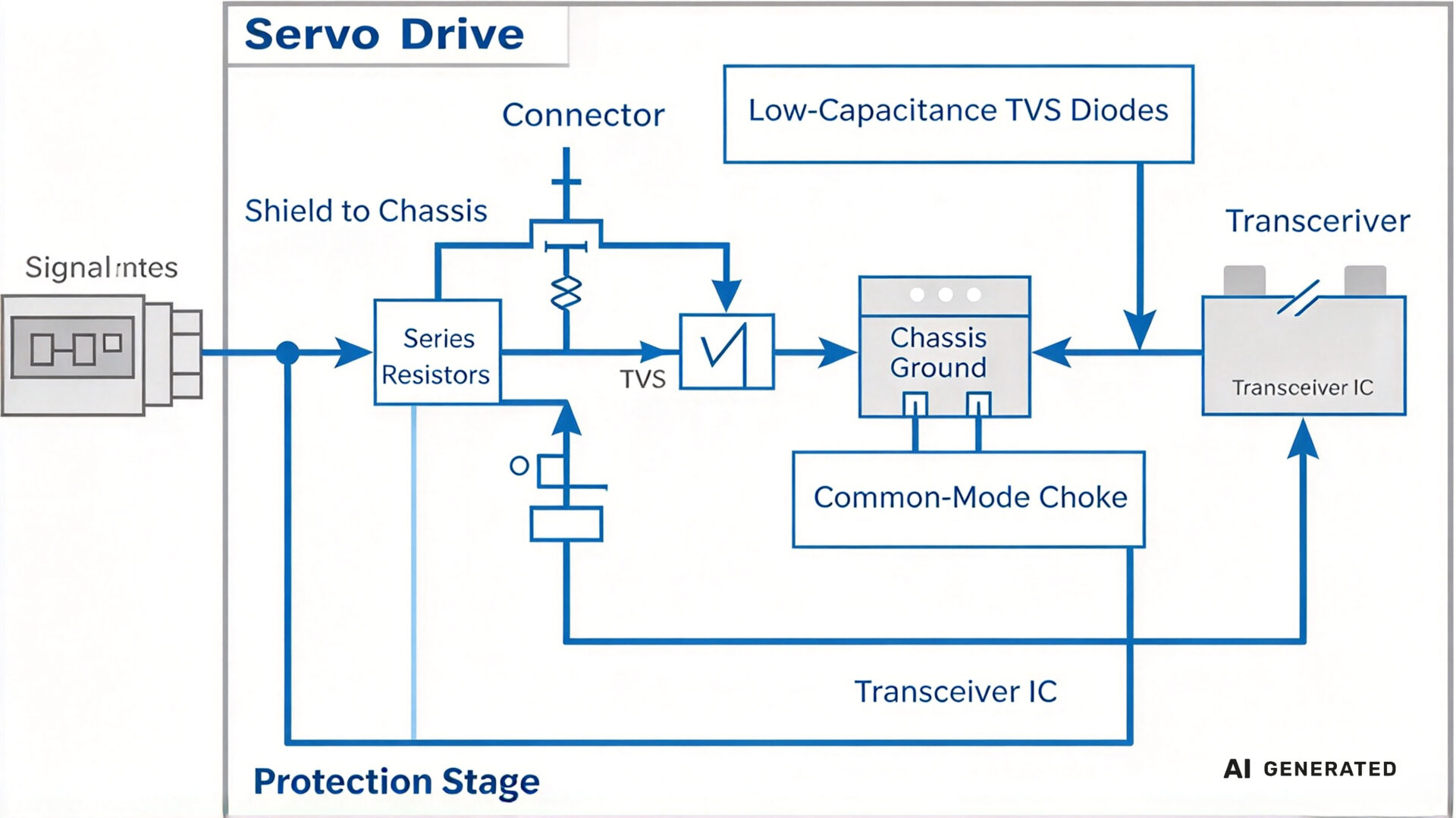
ESD and surge enter through connectors: encoder feedback (often a shielded multi-pin connector), communication ports (RS-485, CAN, Ethernet), digital I/O, and the DC auxiliary supply. If the protection device placed after a long trace from the connector, the trace inductance raises the clamping voltage at the IC, and the IC sees a transient that the TVS was supposed to remove.
Field experience and published design guidance converge on the same rule: the protection device must be placed as close as possible to the connector, with the trace from the connector to the protection device kept short and direct. The protected trace then runs to the transceiver.
2.2 Ground pollution between power, digital, and analog domains
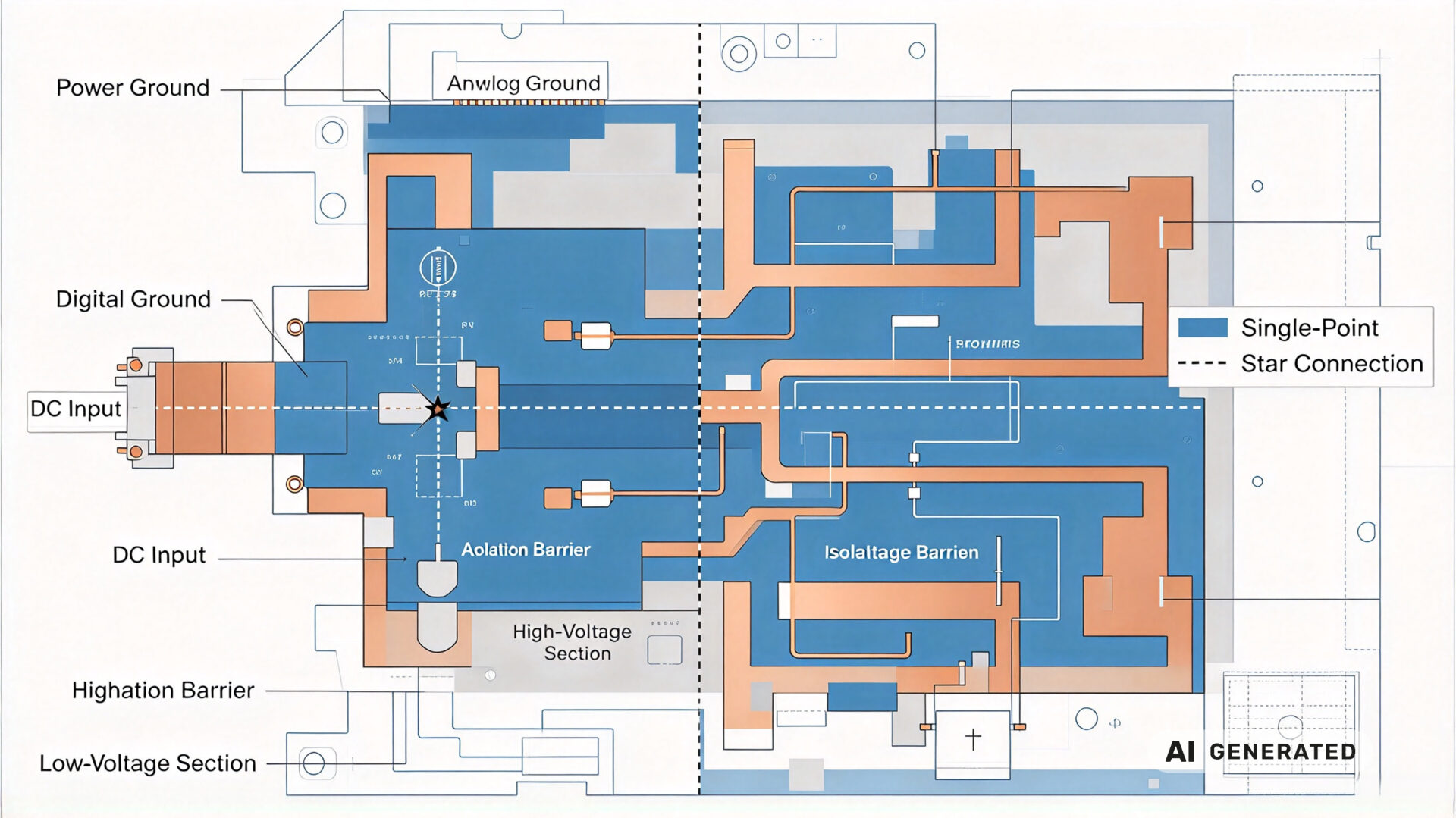
A servo drive PCBA contains at least three ground domains: power ground carrying IGBT/MOSFET switching currents, digital ground for the DSP/MCU and communication, and analog ground for current sensing and encoder signal conditioning. If these share a single copper pour, the switching di/dt develops a voltage difference across the ground plane, and that difference appears as common-mode noise at the analog front-end.
The corrective approach is physical partitioning: separate copper pours for power, digital, and analog ground, joined at a single point—typically near the DC input or the isolation barrier—through a ferrite bead or a 0Ω link. Multiple stitching vias between the domains defeat the purpose, because they create parallel paths for the noise.
3. PCBA-level measures that make the difference
The measures below are not new, but their execution determines whether the drive passes at the first attempt or requires a layout respin.
3.1 Protection stage placement and component selection
For ESD at communication and encoder connectors, the standard arrangement is a series resistor (22–100Ω) followed by a low-capacitance TVS to chassis ground, placed at the connector. The series resistor limits the current into the transceiver; the TVS clamps the voltage; the low capacitance preserves signal integrity at encoder frequencies.
For surge on the DC auxiliary input and the mains input, the protection stage is typically a varistor or TVS with a surge rating above the test level, followed by a common-mode choke and a bulk capacitor. The varistor voltage must be selected above the maximum continuous operating voltage but low enough to clamp before the downstream components exceed their ratings.
3.2 Layout and grounding rules
Three layout rules matter more than any others for ESD and surge:
- Protection at the port, return to chassis: The TVS return must connect to chassis ground through a short, wide trace or a dedicated ground plane, not to the digital ground.
- Keep the protected trace away from the unprotected trace: After the protection device, the trace must not run parallel to the incoming line, or the transient will couple across.
- Shield bonding: The connector shield must be bonded to chassis with a low-impedance connection (360° if possible). A single-wire “pigtail” connection turns the shield into an antenna.
3.3 Isolation coordination
Servo drives use reinforced isolation between the high-voltage power stage and the low-voltage control side. The isolation barrier is also an EMC boundary: surge and ESD currents must not allowed to bridge it through a shared ground or a shared protection return. The isolated gate driver, the isolated encoder interface, and the isolated communication transceiver must each have their protection referenced to the correct side of the barrier.
For PCBA manufacturing, this means the assembly drawing must specify the isolation barrier clearly, and the test fixture must verify isolation withstand after assembly—not only at the design stage.
4. How TPS industrial control PCBA services support EMC-first manufacturing
TPS Elektronik is an EMS provider with a power-electronics engineering team and 25 years of experience in power conversion and control hardware. The PCBA service scope covers SMT and THT assembly, inspection, and test, with an engineering interface that reviews EMC risk before the layout is released.
4.1 DFM review focused on EMC risk
The DFM review is the first control point. TPS engineers check the protection-stage placement, the ground partitioning, the connector shield bonding, and the isolation barrier against the schematic and the layout. The output is a list of actionable changes before tooling and assembly, not after the first EMC failure.
4.2 Assembly, inspection, and protection integrity
ESD and surge performance depends on the physical integrity of the protection components and their solder joints. A TVS with a voided solder joint behaves like no TVS at all. TPS assembly and inspection processes—including AOI and functional test—are configured to verify that protection components are present, correctly oriented, and properly soldered.
4.3 Documentation for the certification file
For the drive’s technical file and the EMC test report, the PCBA manufacturer’s documentation should include the assembly drawing with the protection stage marked, the bill of materials with the surge/ESD ratings of the protection devices, and the inspection records. TPS provides this documentation as part of the PCBA delivery, so the panel builder or OEM can reference it during certification.
5. RFQ checklist for EMC-critical servo drive PCBA
To streamline quotation and engineering review for an industrial control pcba with surge and ESD requirements, provide the following information:
- Immunity targets: ESD contact and air discharge levels, surge level and port (mains, DC auxiliary, signal), and the applicable product standard (e.g., IEC 61800-3 category)
- Port list: Encoder feedback, communication (RS-485/CAN/Ethernet), digital I/O, and DC auxiliary input, with connector types
- Protection schematic: TVS/varistor part numbers and ratings, series resistors, common-mode chokes, and the intended ground reference for each protection device
- Ground partitioning: Power, digital, and analog domains, and the intended single-point connection
- Isolation barrier: Voltage rating, creepage/clearance requirement, and the isolation standard
- PCB stack-up: Layer count, copper thickness, and any impedance-controlled traces
- Test requirements: Whether the PCBA supplier performs functional test and protection verification, and the test coverage
- Documentation: Assembly drawing, BOM with protection ratings, inspection records, and traceability
- Volume and schedule: Prototype, pilot, and series quantities
Providing these details reduces clarification cycles. TPS’s engineering team can support protection-stage review, ground partitioning, and test coverage definition as part of the RFQ process.