

System integrators, test engineers, and procurement teams in semiconductor equipment manufacturing rarely fail because they lack an I-V measurement instrument. They lose time—and budget—when measurement noise, leakage currents. Or instrument drift corrupt device characterization data, forcing repeated test runs and delaying product qualification.
TPS Elektronik’s precision voltage current source integration services built to eliminate that risk: shielded test fixture design, guarded low-current measurement architecture. And validated SMU configurations that deliver repeatable I-V curves from first silicon to production test.
1. The customer challenge: accurate device characterization for advanced semiconductor nodes
A European semiconductor equipment manufacturer approached TPS Elektronik with a recurring problem: their existing test bench configuration produced I-V curves with sufficient resolution for standard silicon devices but failed to resolve sub-picoamp leakage currents in wide-bandgap semiconductor components—specifically GaN and SiC power devices. The measurement noise floor of their current setup exceeded the gate leakage specification of the devices under test.
The customer required a precision voltage current source capable of sourcing and measuring at fA-level resolution while maintaining voltage accuracy better than 0.02% across a ±200 V range. Their existing semiconductor I-V measurement source was a combination of a programmable power supply and a separate electrometer. Which introduced ground-loop noise and required lengthy cable reconfiguration between test phases.
For the procurement team, the challenge was equally clear: the existing setup consumed 40 minutes per device for complete I-V characterization. Which limiting throughput and increasing the cost per characterized die. A device characterization source that could reduce this time while improving measurement confidence was the commercial requirement.
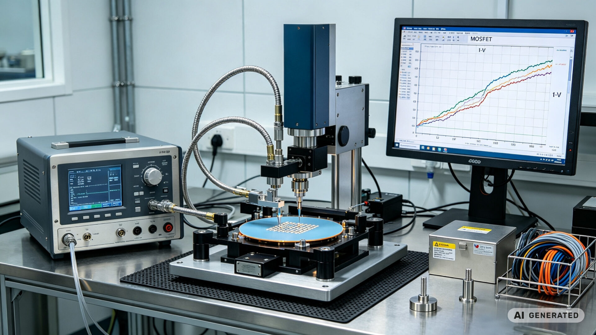
2. I-V curve tracing fundamentals: what precision voltage current source brings to the bench
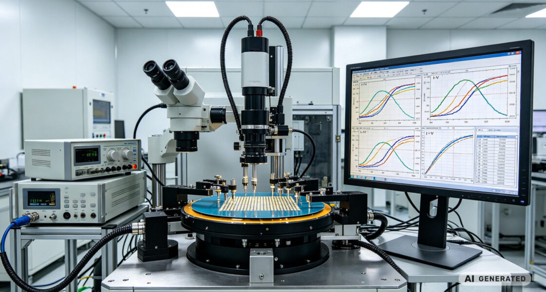
I-V curve tracing is the foundational measurement for semiconductor device characterization. It reveals threshold voltage, transconductance, on-resistance, leakage current, and breakdown behavior—parameters that determine whether a device meets its specification. The quality of the measurement depends almost entirely on the quality of the source and measurement instrument.
2.1 Why a precision source measure unit outperforms separate instruments
A precision source measure unit (SMU) integrates voltage sourcing, current sourcing, voltage measurement, and current measurement in a single instrument with a unified control loop. This integration eliminates the timing skew and ground-loop noise that occur when separate instruments used.
For transistor curve tracing source applications, the SMU’s four-quadrant operation allows it to source or sink current while measuring voltage. Which essential for characterizing devices in both forward and reverse bias. The precision SMU semiconductor test configuration at TPS was specified with:
- Current resolution down to 10 fA for gate leakage measurements
- Voltage source accuracy of ±0.015% + 1 mV at 20 V range
- Four-quadrant operation for forward and reverse device characterization
- Built-in sweep and list mode for automated I-V curve generation
- Triaxial output connectors for guarded low-current measurement
2.2 Low-current measurement challenges and the guarding solution
Low current semiconductor test at the femtoamp level requires more than a sensitive ammeter. Leakage currents from cable insulation, test fixture contamination. And ambient electromagnetic interference can all exceed the device leakage current being measured. The guarding technique—maintaining a conductive enclosure at the same potential as the sensitive signal path. Which reduces these leakage currents by orders of magnitude.
TPS designed a guarded test fixture with triaxial connectors and a guard ring surrounding the device under test. This fixture, combined with the SMU’s triaxial output architecture. Which reduced the measurement noise floor from approximately 50 pA to below 1 pA—sufficient to resolve the gate leakage of the customer’s GaN devices.
For diode leakage test PSU applications, the same guarding principles apply. The SMU sources a reverse voltage across the diode and measures the resulting leakage current, with the guard circuit eliminating parallel leakage paths through the test board.
TPS’s experience with precision electronic assembly for test applications is documented in the precision CNC machining guide and the EMS CNC milling prototype-to-production resource.
3. The TPS solution: integrated precision source measure unit deployment
TPS Elektronik approached the customer’s challenge as an integrated measurement system problem, not a component sourcing exercise. The solution combined precision SMU selection, custom test fixture design and fabrication, and validated measurement procedures.
The deployment included:
- SMU specification and validation: A precision source measure unit with 10 fA current resolution and four-quadrant operation was specified and validated against the customer’s device characterization requirements. The instrument’s sweep mode was configured for linear and logarithmic I-V curve generation.
- Guarded test fixture design: TPS designed a custom test fixture with triaxial connectors, guard rings, and shielding enclosure. The fixture was fabricated using TPS’s EMS CNC milling service, integrating precision machining with electronic assembly.
- Measurement procedure validation: TPS engineers developed and documented the I-V sweep procedures, including settling time optimization, compliance limit configuration, and remote sensing calibration.
- Integration with existing test workflow: The SMU was integrated into the customer’s existing semiconductor parameter analyzer software environment. With SCPI command set configuration for automated test sequencing.
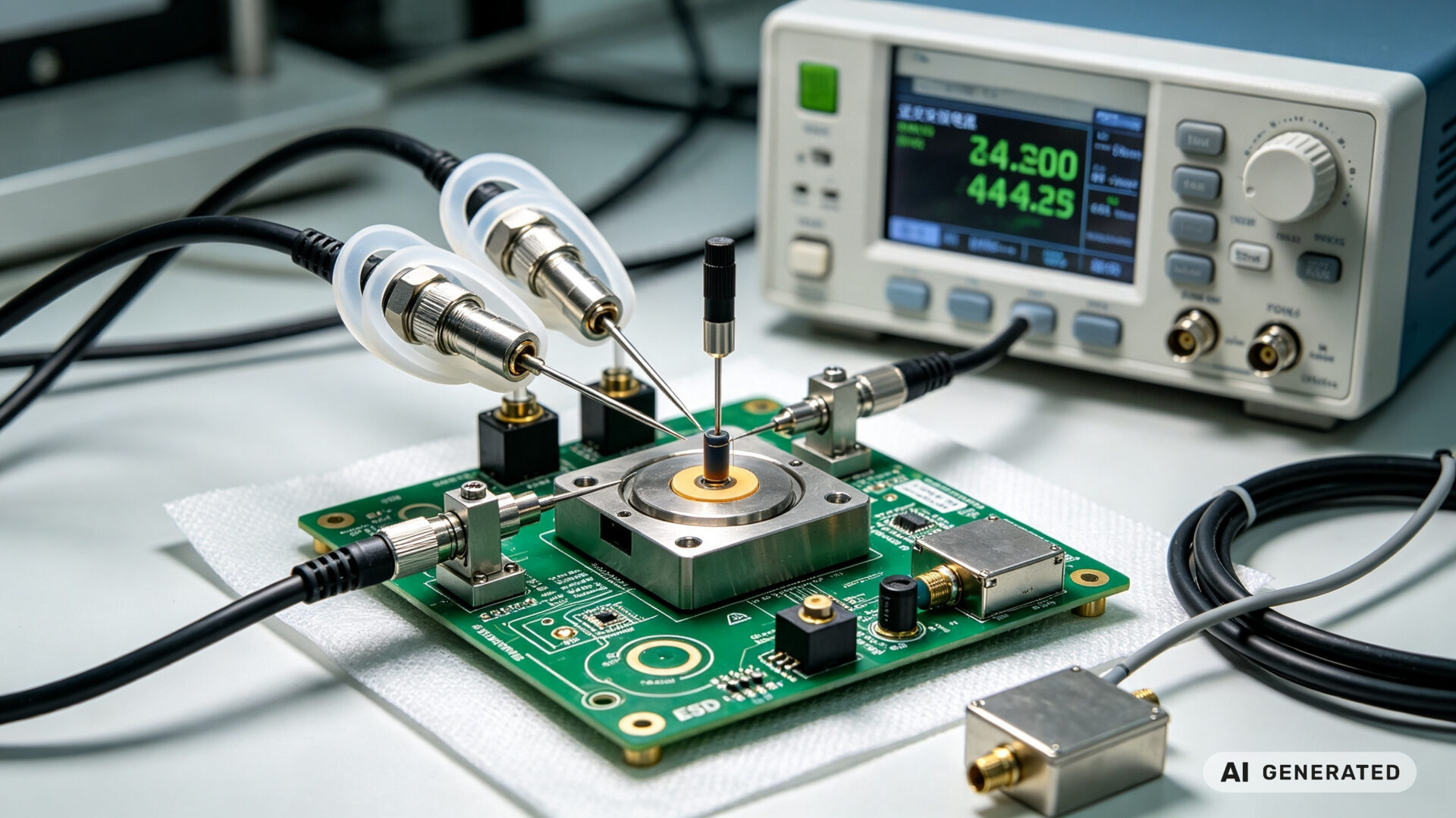
For wafer level characterization source applications, TPS specified a probe card interface compatible with the SMU’s triaxial output. Which enabling direct measurement at the wafer level without cable reconfiguration. This reduced setup time per device from 40 minutes to under 12 minutes.
4. Measured results and customer outcome
The integrated precision SMU and guarded fixture solution delivered measurable improvements across all three customer requirements:
- Measurement noise floor: Reduced from approximately 50 pA to below 1 pA, enabling accurate gate leakage characterization of GaN and SiC devices.
- Characterization time per device: Reduced from 40 minutes to under 12 minutes through integrated sweeping, automated data logging, and eliminated cable reconfiguration.
- Measurement repeatability: Improved to better than 0.5% variation across repeated I-V sweeps on the same device. Which validated against the customer’s reference measurements.
The customer subsequently deployed the TPS-validated configuration across three additional test benches, standardizing their semiconductor characterization workflow on the same precision SMU platform.
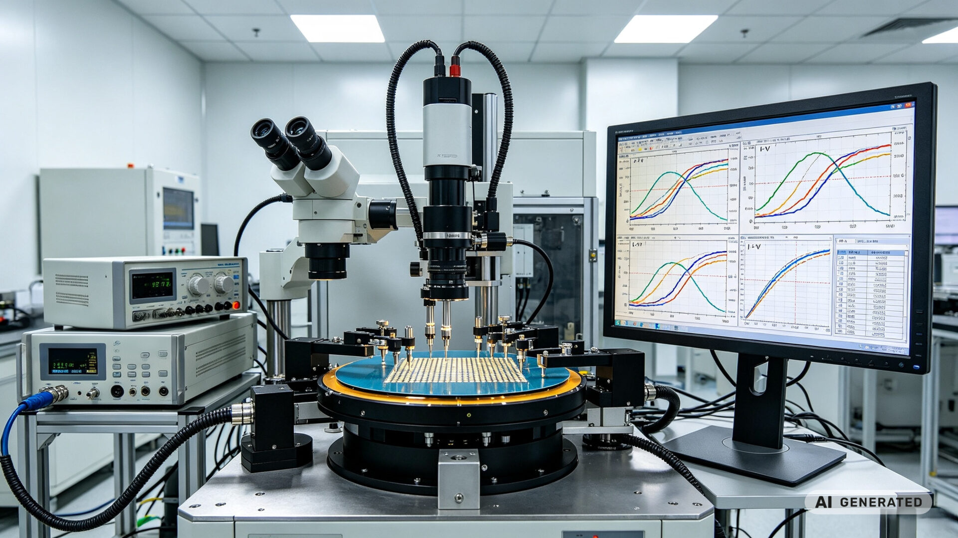
This project reflects TPS’s broader approach to precision electronic assembly and test system integration. The types of milling machine guide and CNC milling machine options resource detail the machining capabilities that support custom test fixture fabrication.