Key Takeaways
- Common PCB components include resistors, capacitors, inductors, diodes, transistors, and integrated circuits (ICs) in through-hole (THT) and surface-mount (SMT) packages.
- SMT enables very high component density (e.g., 0201 resistors at 0.6 mm × 0.3 mm), while through-hole parts offer superior mechanical strength for connectors and high-power devices.
- Component selection should consider electrical specs, package type, operating temperature (often −40 °C to +125 °C), and available board space.
- Modern automated assembly can reach up to ~80,000 components per hour with placement accuracy around ±25 µm, depending on equipment, design, and process setup.
- Sourcing from authorized distributors (e.g., Digi-Key, Mouser, Arrow, Avnet) supports traceability and helps reduce counterfeit risk.
Introduction to Electronic Components on PCBs
Electronic components are the building blocks that turn a bare printed circuit board into a working device—from wearables to industrial controls. Mounted on fiberglass substrates with copper traces, they create circuits that process signals, manage power, and execute computational tasks.
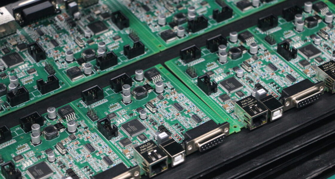
The transition from through-hole to SMT has enabled miniaturization and performance gains. Today’s multilayer PCBs can host thousands of components in a footprint smaller than a credit card, with some packages as small as 01005 (≈ 0.4 mm × 0.2 mm). Understanding how components and PCB assembly interact is essential for designing reliable, manufacturable electronics.
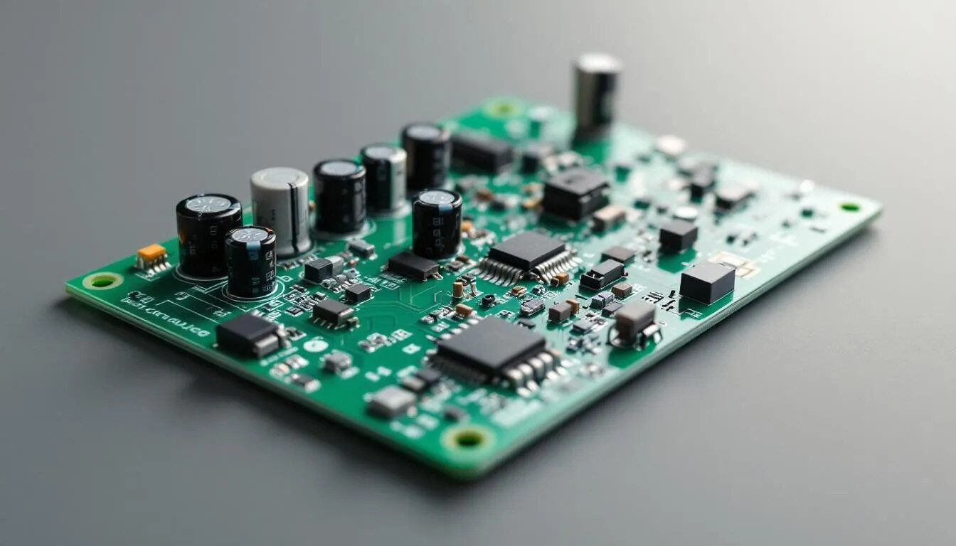
Types of Electronic Components for PCBs
Component choice depends on application requirements, available PCB area, and the assembly process. Broadly, components are passive or active.
Passive Components
Resistors (carbon film, metal film, thin-film/chip) are ubiquitous. SMT sizes range from 2512 down to 0201 (0.6 mm × 0.3 mm). Typical values span ~1 Ω to 10 MΩ, with tolerances as tight as ±0.1% for precision designs.
Capacitors provide energy storage and filtering. Ceramic MLCCs dominate SMT designs thanks to size and high-frequency behavior; electrolytics handle bulk energy; tantalum offers high volumetric efficiency. Common ranges: ≈ 1 pF to 10,000 µF.
Inductors (ferrite core, air core, chip) store energy and filter noise, from ≈ 1 nH to 100 mH—essential in switch-mode power supplies, RF, and EMI suppression.
Crystal oscillators and resonators supply timing references—from 32.768 kHz RTC crystals to tens of MHz for high-speed digital systems.
Active Components
Diodes (signal, power, Schottky, Zener) appear in SOD/DO/SMA packages. Schottky types exhibit low forward drop (often ~0.2–0.3 V), and Zeners provide regulated reference voltages.
Transistors include BJTs and FETs across SOT-23, DPAK/TO-220, QFN, and BGA. Modern power MOSFETs can handle high currents with very low R<sub>DS(on)</sub>, enabling efficient power stages.
Integrated circuits range from op-amps and regulators to microcontrollers, FPGAs, and SoCs, in DIP, QFP, QFN, and high-pin-count BGAs. Power-management ICs include high-efficiency switching regulators, low-noise LDOs, and battery-management solutions.
Component Mounting Technologies
The mounting approach impacts density, cost, throughput, and reliability.
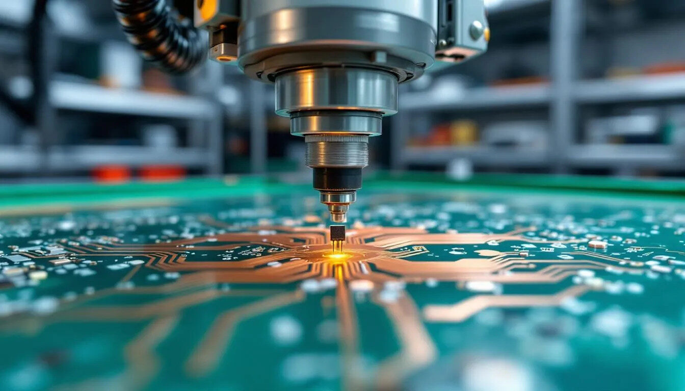
Surface-Mount Technology (SMT)
SMT places components directly on pads without drilled holes. Packages span from 01005 passives to high-pin-count BGAs. Benefits include:
- Significant space savings vs. through-hole
- High throughput via automated pick-and-place
- Short interconnects that can improve high-frequency performance
Typical process steps:
- Solder paste printing via laser-cut stencils (fine-pitch stencils often ~0.10 mm thick)
- Placement (throughputs up to ~80k cph; typical accuracy around ±25 µm)
- Reflow soldering with lead-free peak zones commonly ~240–260 °C (profile depends on paste and design)
Through-Hole Technology (THT)
THT inserts leads through drilled holes (commonly ~0.6–3.2 mm) for robust mechanical anchoring—favored for connectors, transformers, and high-power parts, and useful for prototyping and field service.
- Wave soldering typically operates near ~250 °C.
- Selective soldering targets THT joints in mixed-technology assemblies.
- Manual soldering supports low-volume/prototype work (use temperature-controlled tools and appropriate flux).
Most production uses mixed assembly: SMT for density and THT where strength or serviceability is required.
Component Selection and Sourcing
Selection balances performance, reliability, availability, and cost.
- Electrical & thermal: voltage/current ratings, frequency response, temperature coefficient, junction/ambient limits.
- Package & layout: available PCB area, creepage/clearance, thermal dissipation, assembly capability.
- Lifecycle & availability: prefer parts with clear longevity data; plan for second sources; consider last-time-buy and redesign triggers.
- Sourcing: authorized distributors (e.g., Digi-Key, Mouser, Arrow, Avnet) provide traceability, datasheets, and parametric search tools—helping lower counterfeit risk and simplifying compliance.
Build resilience with approved-vendor lists, alternate BOMs, and buffer stocks where appropriate.
PCB Design Considerations for Components
Design choices strongly influence manufacturability and reliability.
- Footprints: follow IPC-7351 (or manufacturer-recommended land patterns).
- Placement & spacing: respect pick-and-place, reflow, and inspection constraints; align orientations to aid AOI.
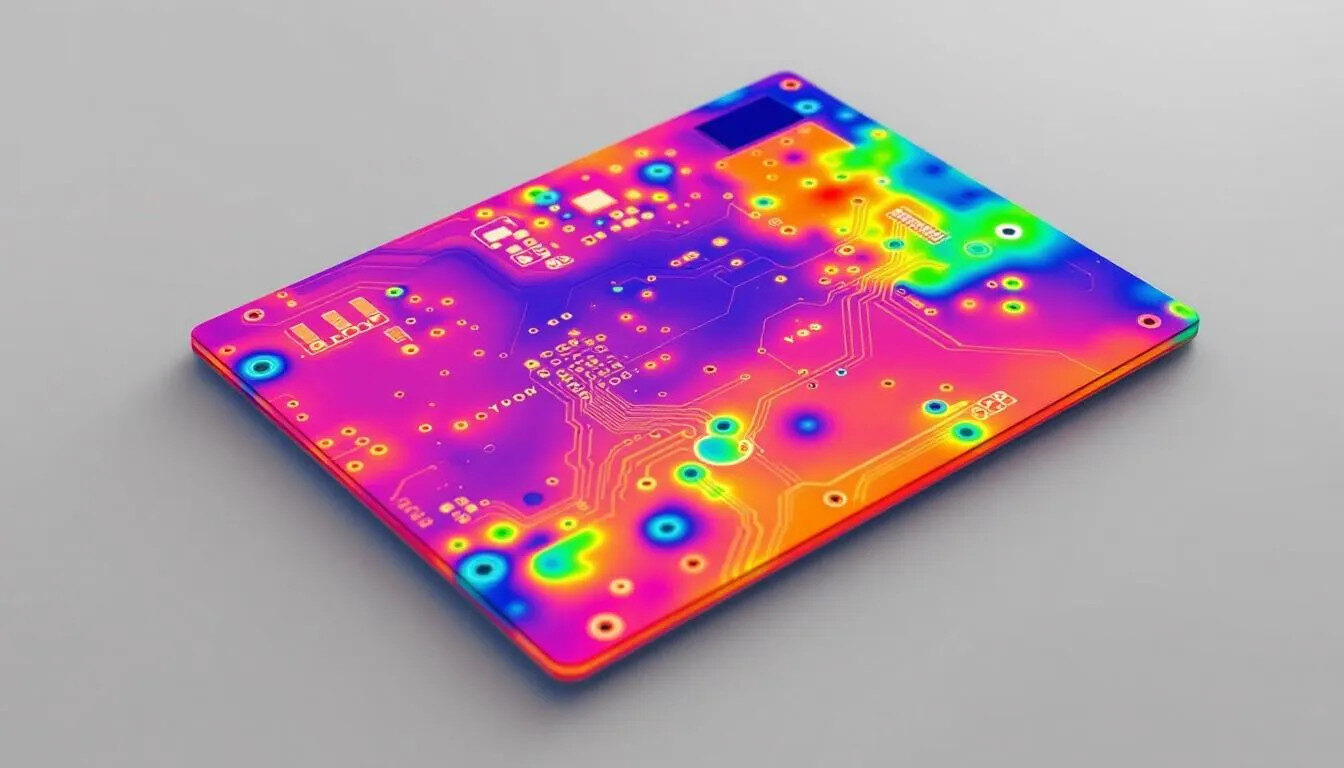
- Thermal management: use copper pours, thermal vias, heatsinking areas, and spacing to avoid hot-spot coupling; add thermal relief where needed.
- Signal integrity & EMI: controlled-impedance routing, continuous reference planes, short return paths; isolate sensitive analog from noisy switchers; decouple ICs locally (often within 2–5 mm).
- Power distribution: size traces/planes for current and temperature rise; consider copper thickness and via current sharing.
- DFM: observe minimums to avoid bridges; add global and local fiducials; standardize orientations to streamline assembly.
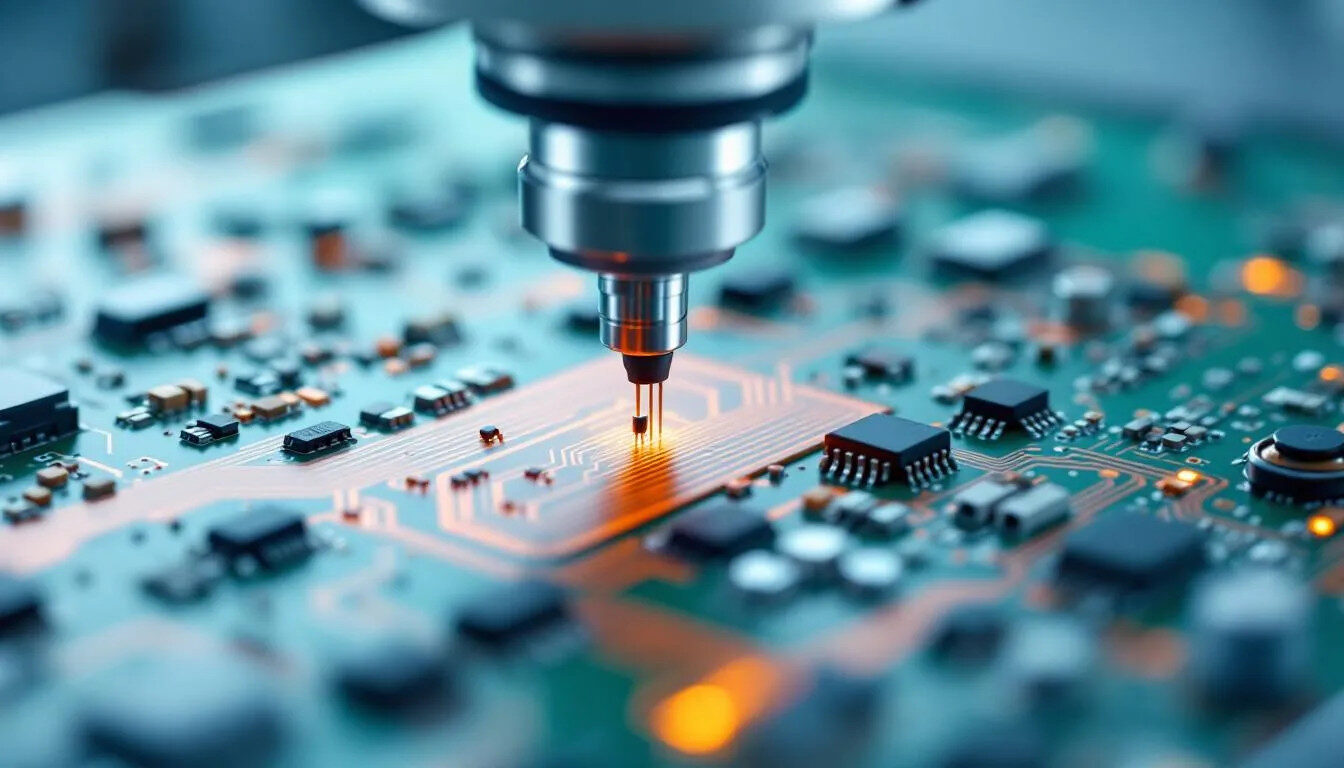
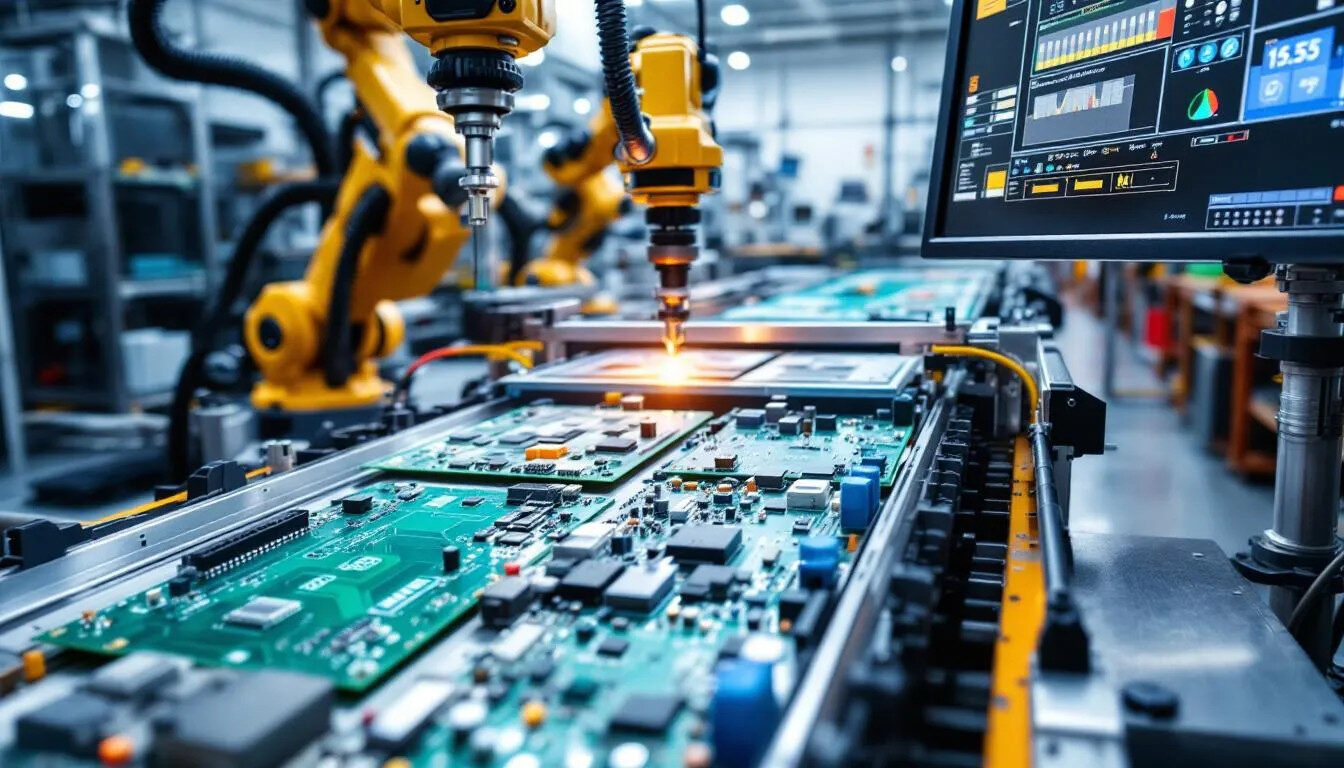
Assembly Process for Electronic Components
From bare boards and reels to finished assemblies:
- Solder paste printing
Optimize stencil design, aperture ratios, and printing parameters (typical squeegee force ≈ 22–67 N / 5–15 lbf). Use SPI to verify deposit volume and shape. - Pick-and-place
Maintain accurate package libraries (x/y/θ, height, vision). Modern machines can place at high speed while preserving fine-pitch accuracy. - Reflow soldering
Tune preheat/soak/reflow/cool zones to paste specs (e.g., SAC305 peak ~245 °C). Aim for adequate wetting without exceeding component thermal limits. - THT insertion & soldering
Use selective solder for mixed assemblies; protect heat-sensitive SMT with pallets or masking. - Rework & hand soldering
Apply controlled temperature, appropriate tip geometry, flux selection, and ESD-safe practices.
Quality gates (SPI, placement verification, post-reflow inspection) catch defects before test and pack-out.
Testing and Quality Control
Robust test strategies validate function and reliability before shipment.
- AOI: detects missing/misaligned parts and solder defects; typical repeatability around ±50 µm with multi-angle lighting.
- X-ray: essential for hidden joints (BGA/QFN) to assess voiding, opens, and bridges.
- In-Circuit Test (ICT): bed-of-nails fixtures verify component values and nets (e.g., resistor within tolerance, shorts/opens).
- Functional test: confirms behavior under defined operating conditions (power draw, timing, interfaces, limits).
- Environmental stress: temperature cycling (e.g., −40 °C to +85 °C), humidity per IPC methods, and vibration profiles representative of transport/use.
- SPC & CAPA: track yields and defect modes; drive continuous improvement across print, place, and reflow.
Final inspection, electrical test, and packaging complete the manufacturing flow.
Electronic component selection and PCB assembly are at the heart of every reliable electronic product. By combining well-chosen components, robust design practices, and precise manufacturing processes, engineers can achieve consistent quality and long-term performance.
Whether for prototypes or large-scale production, attention to component quality, sourcing, and testing ultimately determines the success of any electronic system.
Frequently Asked Questions
What is the smallest electronic component commonly mounted on a PCB?
01005 passives (≈ 0.4 mm × 0.2 mm) are among the smallest widely used. They require advanced equipment, tight process control, and careful DFM.
How do you prevent ESD damage during assembly?
Use an ESD control program: grounded workstations, wrist straps, ESD garments/footwear, ionizers, and humidity control (often ~45–65%). Store and handle parts in ESD-safe packaging, and ensure all tools are properly grounded.
What are the key differences between lead-free and leaded solder?
Lead-free alloys (e.g., SAC305: Sn96.5/Ag3.0/Cu0.5) typically need higher peak temperatures (~245 °C) versus Sn63/Pb37 (~215 °C). Lead-free joints often look more matte and can be more susceptible to tin whiskers; they are favored for RoHS compliance and environmental reasons.
How do you size PCB traces for current?
Capacity depends on width, copper weight, environment, and allowed temperature rise. As a rough starting point, ~1 mm width of 1 oz copper might carry around 2–3 A for a ~10 °C rise. For design, use IPC-2221/IPC-2152 methods or trusted calculators, and consider copper pours or parallel paths for higher currents.
How can you detect counterfeit components?
Combine visual checks (markings, date codes, packaging), electrical verification of key parameters, and X-ray for internal structure on critical parts. Prefer authorized channels with traceability and avoid unusually low-priced stock from unknown sources.


