How integrated PCB and software development helps bring compliant, reliable medical devices and industrial systems to market faster.
Overview
Electronics and healthcare are converging fast. From connected diagnostics to industrial control systems, strong outcomes depend on two disciplines working in sync: professional PCB design and medical-device software engineering.
This article explains how integrated teams shorten development cycles, reduce rework, and support compliance — without hype.
Why the Demand Is Rising
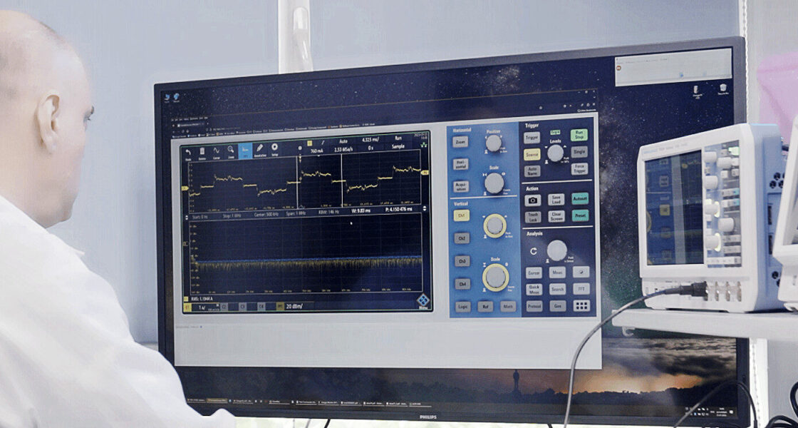
Software now powers monitoring, connectivity, and data analysis in healthcare and beyond. At the same time, hardware complexity is increasing — with dense layouts, RF challenges, low-power requirements, and safety constraints.
Reliable products require coordinated decisions across the stack — from system architecture to PCB layout, firmware, cybersecurity, and usability.
Compliance note: In regulated contexts, development should align with applicable standards and processes (e.g., quality management, risk management, and software lifecycle standards). The specifics depend on device classification, market, and product scope.
What a Capable Partner Delivers
An experienced development partner brings more than tools — they bring structure, verification, and accountability across every stage.
PCB Design & Layout
- Requirements capture, schematic design, and DFM/DFT checks
- Stack-up planning, impedance control, and high-speed/RF layout constraints
- Prototype bring-up and functional testing
- Manufacturing documentation and bill of materials (BOM) hygiene
Embedded Software & Device Firmware
- Architecture and interface design (drivers, middleware, connectivity)
- Robust update concepts (bootloader/DFU) and error-handling mechanisms
- Sound security hygiene — least privilege, secure key handling at rest and in transit
Integration & Verification
- Hardware–software co-design to detect issues early
- Functional tests, boundary conditions, and regression suites
- Pre-compliance checks (EMC, safety, wireless) to minimize late-stage surprises
Manufacturing & Assembly (When End-to-End Is Needed)
- Prototype-to-small-batch support and supplier coordination
- Test fixtures and documentation for seamless volume-production handover
Selecting PCB and Software Services (Without the Buzzwords)
With many providers in the market, focus on evidence over adjectives. Look for partners that demonstrate:
- Relevant references: Experience with similar device classes, interfaces, and constraints
- Processes: Documented development and change control procedures
- Verification depth: Clear proof of how requirements are validated and met
- Design for manufacture: Yield optimization, test coverage, and supplier readiness
- Transparent costing: Effort drivers clearly explained (layers, speeds, RF, test)
- Proximity when useful: Local collaboration can accelerate reviews; remote setups work well when supported by strong tools and regular communication
Common Challenges — and Practical Ways to Address Them
Even experienced teams face recurring technical and organizational challenges. A few of the most common include:
- Network topology vs. hardware constraints: Balancing bandwidth, isolation, and security with PCB realities such as return paths, EMI, and thermal management.
- High-speed signals in tight spaces: Early stack-up planning and constraint-driven routing can dramatically reduce respins.
- Security as a feature, not an afterthought: Integrate threat modeling and key management into the initial architecture.
- Total cost visibility: Real costs stem from complexity — layer count, component selection, and test depth — not merely day rates.
Cost and Sourcing — Keeping It Real
Global sourcing options — including those in Asia — can offer attractive lead times and competitive costs for certain project scopes.
However, for regulated products, it’s essential to factor in communication overhead, documentation requirements, and audit readiness, not just unit pricing.
A hybrid model — with a local lead handling requirements and verification, and global partners managing fabrication or assembly — often delivers the best balance of speed, quality, and compliance.
Key Takeaways
- Coordinated PCB and software design ensures faster, safer product development.
- Compliance and verification are the foundation of long-term reliability.
- A hybrid sourcing model can balance speed, cost efficiency, and quality outcomes.
Conclusion
Integrated hardware–software development reduces risk and improves product readiness.
By emphasizing process, verification, and manufacturability — rather than buzzwords — teams can deliver reliable, scalable, and compliant solutions that are easier to certify, maintain, and bring successfully to market.


