Key Takeaways
- Buck and boost converter design success hinges on clean requirements, correct topology choice, and disciplined buck-boost converter PCB design—layout quality can make or break efficiency and EMI performance.
- Use first-order buck-boost converter design equations to size L and C, then refine with loss models and thermal simulation. Maintain a reproducible buck-boost converter calculation worksheet for every project.
- For robust products, verify both the analog power stage and the software stack: handle hard-switching power-supply artifacts, and apply the circuit breaker design pattern in services that control your power devices.
- Good R&D practice spans electronics and software—from DC-DC buck-boost converters to microservices resilience and even sensor fusion (e.g. an analog integrated 2-D optical flow sensor feeding a motor controller).
- Document assumptions, measure early, and iterate. This significantly increases the likelihood that your converter systems pass compliance and scale in production.
In development, power and software reliability meet at the product boundary. This guide covers buck-boost converter circuit fundamentals, a practical design flow for DC-DC implementations, PCB layout pitfalls to avoid, and where patterns like the circuit breaker design pattern in microservices keep your control plane healthy while hardware operates under stress.
Step-by-Step: How to Design a Buck Boost Converter
- Specs: Define Vin(min/max), Vout, Iout, ripple targets (ΔIL, ΔVout), and ambient/max case temperatures. This frames the overall design space.
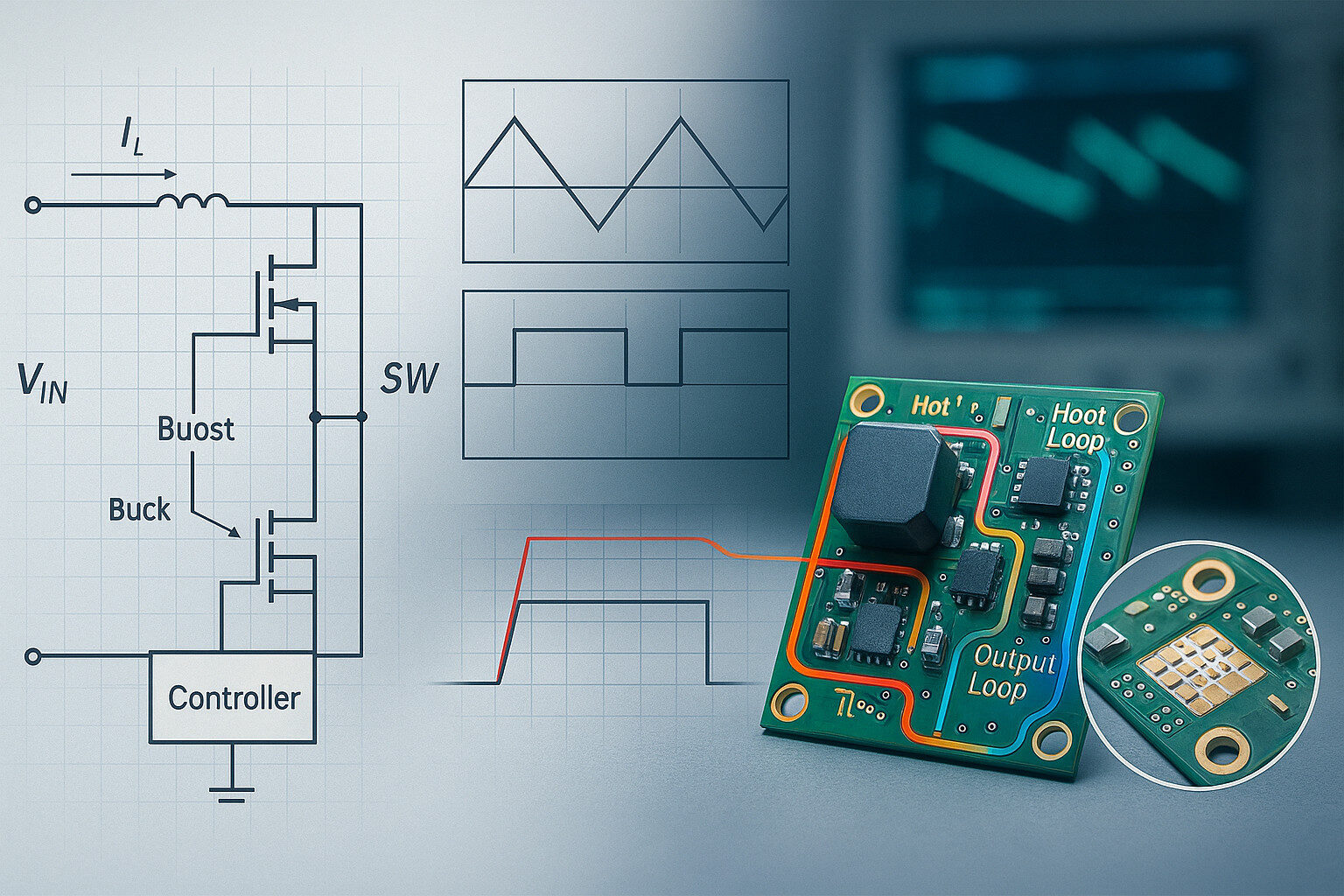
- Topology & control: Choose a suitable topology (e.g. synchronous non-inverting) for wide-range efficiency. Select the switching frequency fsw to balance size versus loss.
- First-cut sizing: Apply core buck-boost design equations (continuous conduction) to estimate L (via ΔIL) and Cout (via ΔVout and ESR). Maintain a traceable calculation sheet.
- Loss & thermal: Model MOSFET conduction and switching losses, diode losses (if asynchronous), and inductor core/copper losses. Iterate until junction temperatures and magnetics meet the thermal budget.
- Compensation & protection: Close the control loop, confirm phase and gain margins, and add OCP/OVP/OTP. Plan line and load transient tests early to validate stability under realistic conditions.

Buck-Boost Converter PCB Design: Layout Rules That Matter
Great schematics can still fail on copper. In buck-boost converter PCB design, shrink the hot loop (VIN–FET–inductor–ground), place input ceramics tight to the switch, and route the sense and compensation network quietly. Pour copper for thermal spreading and stitch with vias under the power devices.
- Loops: Minimize switch and rectifier current loops. Keep the SW node small and away from sensitive traces.
- Grounding: Use star or split analog and power grounds, then join them at the controller ground-sense point.
- Thermals: Connect power-device tabs to internal planes and use thermal vias under FETs and inductors.
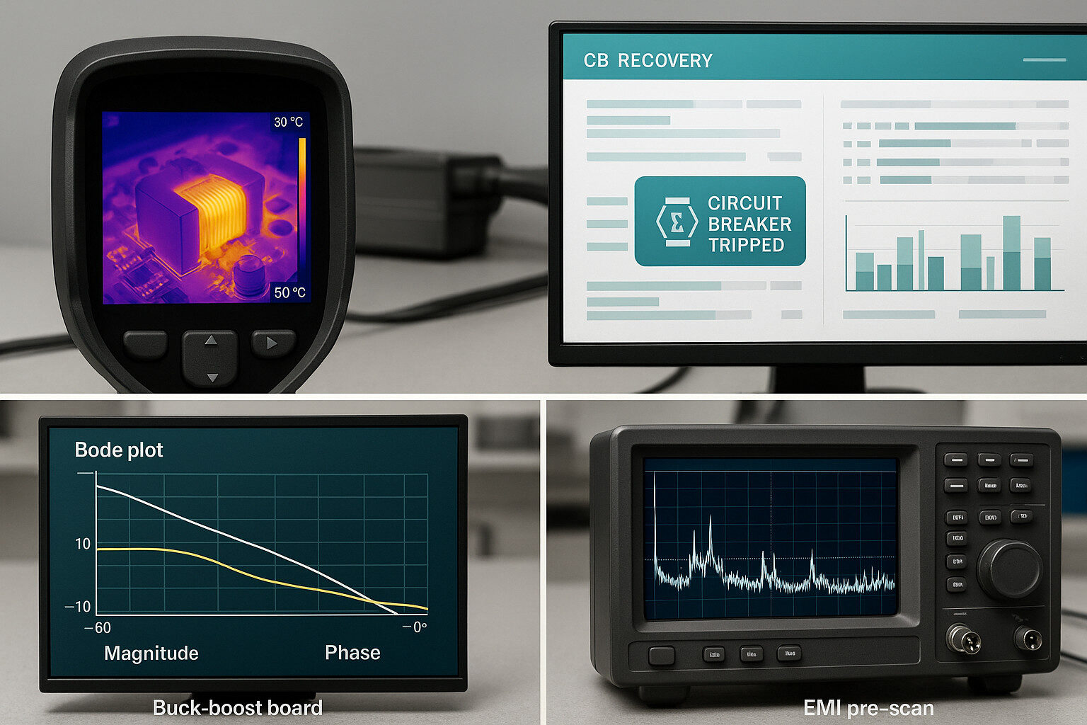
- Probes & Design for Test (DfT): Add Kelvin measurement points for IL and Vout, plus a clean injection loop for Bode testing and frequency-response measurements.

Hard-Switching Power Supplies: Practical Caveats
Many cost-optimized converters are hard-switching power supplies. When power-stage nodes are hard-switched, high dV/dt and dI/dt can increase EMI and stress components. Snubbers, proper dead-time, and gate-drive tuning help tame ringing.
If your product includes a user-facing rocker or mechanical on/off switch—such as in a PC-style power supply at the AC input or 12 V rails—debounce and place it carefully to avoid nuisance resets and unwanted transients.

Worked Example: DC-DC Buck-Boost Converter Circuit Design
This mini example outlines a reproducible DC-DC buck-boost converter circuit design flow used in our lab.
Values shown are illustrative and must be validated for each application.
- Inputs: Vin = 6–16 V, Vout = 12 V @ 4 A, ΔIL ≈ 30 %, fsw = 400 kHz.
- Inductor: Size L from the ripple specification, then select a low-loss inductor considering both core and copper losses.
- Output capacitor: Compute Cout from the allowable output ripple (ΔVout) and ESR.
- Simulation: Simulate line and load steps to verify stability and transient response.
The same flow scales to higher-power designs with thermal derating, thicker copper planes, and additional heatsinking as required.
Controls & Sensing: From Power to Perception
Power converters increasingly sit beside sensors and compute. A common pairing in robotics, for example, is a buck-boost stage feeding a vision MCU and an analog integrated 2-D optical flow sensor. Stable rails and clean ground segregation allow low-level analog signals to coexist with noisy switching power stages.
Reliability Patterns: Circuit Breakers in Hardware & Software
Hardware protection is essential—a circuit breaker is a device designed to interrupt overcurrent and reduce the risk of damage or fire. In parallel, service backends that configure and log converters benefit from adopting the circuit breaker design pattern in software.
This pattern stops cascading failures by opening after repeated errors, then retrying once downstream health recovers. In a typical architecture, it sits in microservices that provide telemetry and configuration APIs, helping prevent failing downstream services from blocking user interfaces, production tools, or HIL benches.
Pair both worlds: robust hardware limits and resilient APIs.

Miniature Circuit Breaker Design & Power Projects
When power stages ship with field-replaceable protection, review miniature circuit breaker design curves (B/C/D trip), ambient ratings, and wiring. At enclosure level, the circuit breaker choice affects inrush behavior, compliance, and safety labeling—especially around battery input stages and pre-charge schemes.
FAQ
Q1. What’s a pragmatic way to design buck-boost converter hardware quickly?
A: Start with a proven controller reference design, perform first-order sizing using standard equations, simulate, then prototype with generous measurement points. Keep a versioned calculation sheet for traceability and efficient design reviews.
Q2. How do I stabilize a noisy layout?
A: Re-route the hot loop, tighten placement of input ceramics, shield or reroute the sense network, and adjust snubbers. Many issues trace back to PCB layout rather than IC selection.
Q3. Are hard-switching power supplies always a bad idea?
A: No. Many designs are hard-switched for cost and size reasons. The key is controlling ringing and emissions through layout, snubbers, and gate-drive tuning. Soft-switching can help but is not mandatory.
Q4. Where does a microservices circuit breaker fit in power products?
A: Typically in telemetry and configuration services. The circuit breaker design pattern prevents failing downstream services from blocking UIs, production systems, or test benches.
Q5. What documentation should ship with a prototype?
A: At minimum: schematic and BOM, circuit design notes, loss and thermal budget, stability plots, and a validated calculation workbook for the DC-DC buck-boost design.
TPS Elektronik can support you along the R&D chain—from buck-boost converter design and compliance support through to embedded firmware and service reliability—so that prototypes are built on a solid foundation and can evolve into scalable products.